| Table 994. TEM images of cobalt silicides.
| Cobalt silicides |
TEM images |
| CoSi2 |
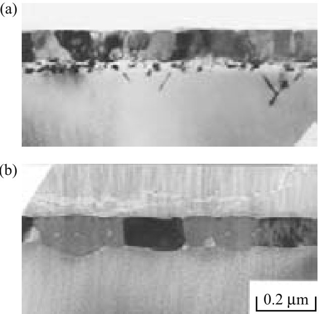
Residual defects formed in ion implanted silicon can be reduced by silicide formation. Figures above show the removal of end-of-range defects by CoSi2 formation in BF+2-implanted (001)Si for samples annealed at: (a) 700°C and (b) 800°C. [1] |
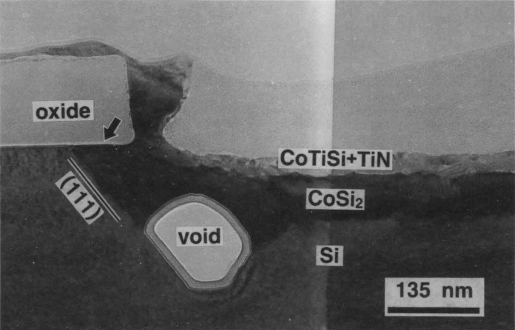
Epitaxial CoSi2 is preferentially nucleated at the Si surface of the lateral encroachment which shows a (111)Si plane due to the lowest interface energy of (111)CoSi2/(111)Si. Before the epitaxial CoSi2 grains fully merged to form a continuous CoSi2 layer, excessive Si atoms diffuse from the Si substrate to the outer layer, thus resulting in the void. [3] |
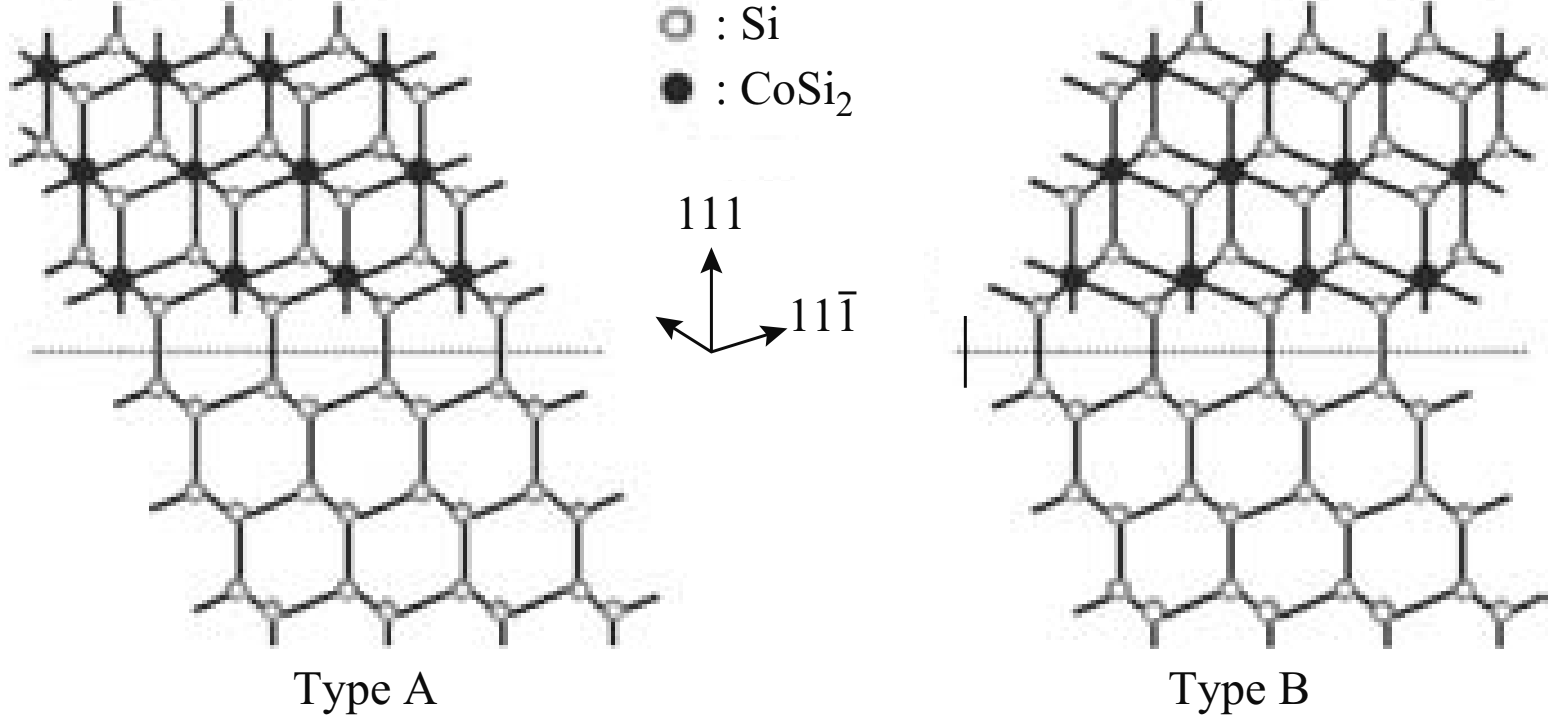
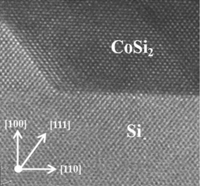
The CoSi2 facets are normally on {111} and {001} Si planes, which have lower free energy than those of other interfaces. For instance, in the figures above, the ball-and-stick models of CoSi2/(111)Si interface with epitaxially (type A) and twin related (type B), respectively, view is down [-110]. [1] |
Co/SiOxNy/Si structure annealed at 500 °C for 1 min in ambient N2. [2] |
[1] Lih J. Chen, Silicide Technology for Integrated Circuits, 2004
[2] Jaesang Lee, Keunwoo Lee, Dongock Kim, Taeyong Park, Honggyu Kim, and Hyeongtag Jeon, Epitaxial CoSi2 formation using an oxynitride buffer layer, J. Mater. Res., 24, 8, 2009.
[3] Jeong Soo Byun, Jeong Min Seon, Kang Shik Youn, Hyunsang Hwang, Jin Won Park and Jae Jeong Kim, Defect Generation during Epitaxial CoSi2 Formation Using Co/Ti Bilayer on Oxide Patterned (100)Si Substrate and Its Effect on the Electrical Properties, J. Electrochem. Soc. 143 L56 (1996).
|
