Chapter/Index: Introduction | A | B | C | D | E | F | G | H | I | J | K | L | M | N | O | P | Q | R | S | T | U | V | W | X | Y | Z | Appendix
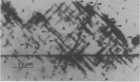
| Figure 2117 shows an example of cathodoluminescence (CL) images. This image was taken from a ZnSe/GaAs heterostructure. The dark-line defects (DLDs) formed primarily along (100) directions ([100] and [010]) in the area (labeled A) photodegraded by an argon laser. Some DLDs marked by arrowheads are misoriented by 5 to 25 degrees from the <100> directions. "M" in the figure marks a misfit dislocation.
Figure 2117. Cathodoluminescence (CL) image taken from a ZnSe/GaAs heterostructure. Adapted from [1]
Table 2117 shows examples of the lattice mismatches between the substrates and epitaxial layers, and the critical layer thickness and the resulting misfit dislocation separation corresponding to complete misfit relaxation for the basal plane interfaces. Table 2117. Examples of lattice mismatches between substrate A and epitaxial layer B, lattice parameter on the basal plane, and critical layer thickness and resulting misfit dislocation separation for a fully relaxed interface.
[1] L. Salamanca-Riba and L.H. Kuo, Observation of [100] and [010] Dark Line Defects in Optically Degraded ZnSSe-Based LEDs by Transmission Electron Microscopy, Journal of Electronic Materials, 25 (2) (1996) 239.
|