Chapter/Index: Introduction | A | B | C | D | E | F | G | H | I | J | K | L | M | N | O | P | Q | R | S | T | U | V | W | X | Y | Z | Appendix
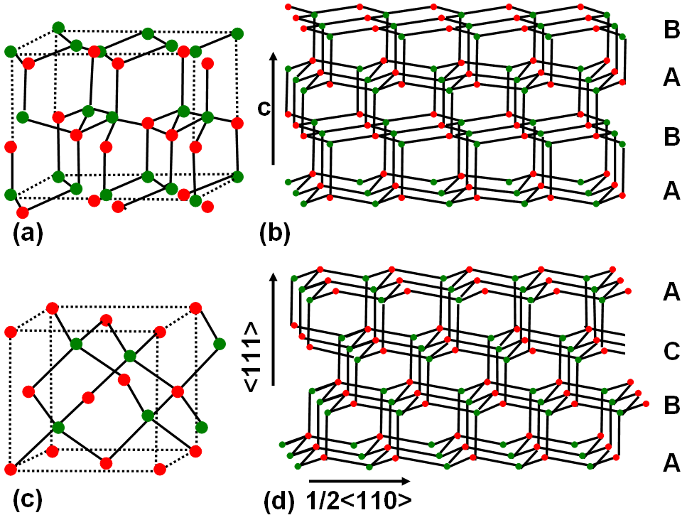
| The atoms in nitride semiconductors are tetrahedrally coordinated with hybrid sp3 orbitals. As shown in Figure 2119, the atomic layers of the nitride semiconductors are arranged in hcp (hexagonal closed packed) planes with alternating sub-layers consisting of Group III and V elements. These layers can be stacked in different ways. For instance, Figure 2119 (a) and (b) shows a configuration in the sequence …ABABAB…, resulting in the hexagonal wurtzite structure (space group P63mc), while Figure 2119 (c) and (d) shows a stacking sequence of the type... ABCABCABC… , resulting in the cubic zincblende crystal structure (space group F-43m). The indices of the stacking planes are {0001} for the hexagonal and {111} for the cubic structures. One example is that GaN cubic zincblende crystal structure can transform into hexagonal wurtzite phase due to annealing.
Figure 2119. Two main types of atomic configurations in the nitride semiconductors. Unit cells for (a) hexagonal wurtzite structure (b) cubic zincblende structure, and (b) and (d) theircorresponding ctystalline layer stacks, respectively. Because of many considerations, the choice of substrates for the growth of nitride semiconducting epilayers is limited to few materials such as SiC, sapphire, and GaAs. Table 2119a lists the lattice properties of the nitride semiconductors and most common substrates used for growth of nitride semiconducting epilayers. Table 2119a. The lattice properties of the nitride semiconductors and most common
Table 2119b. Magnitudes of Burgers vectors of dislocations in nitride semiconductors (in Å).
|