|
Defects in Materials
- Practical Electron Microscopy and Database -
- An Online Book -
|
https://www.globalsino.com/EM/
|
This book (Practical Electron Microscopy and Database) is a reference for TEM and SEM students, operators, engineers, technicians, managers, and researchers.
|
=================================================================================
As an example, Table 2389 lists the electronic properties that are affected by structural disorders in amorphous and crystalline Si.
Table 2389. The electronic properties affected by structural disorders in amorphous and crystalline Si.
Electronic properties |
Structural disorders |
|
Bonding disorder |
Electronic states in band gap
|
Structural defects |
Electronical, metastable states |
Alternative bonding configurations |
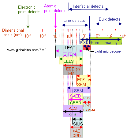
Figure 2389 shows the typical sizes of various material defects and the capability of analytical techniques (See the full names of the techniques at page3928). The lowest levels of the techniques represent their spatial resolutions.
Figure 2389. Typical sizes of various material defects and capability of analytical techniques.
|
=================================================================================
The book author (Yougui Liao) welcomes your comments, suggestions, and corrections, please click here for submission. If you let book author know once you have cited this book, the brief information of your publication will appear on the “Times Cited” page.
|
|