Bond-pad Contamination in IC Devices
- Practical Electron Microscopy and Database -
- An Online Book -

https://www.globalsino.com/EM/  


This book (Practical Electron Microscopy and Database) is a reference for TEM and SEM students, operators, engineers, technicians, managers, and researchers.
 

=================================================================================

In IC devices, fluorine corrosion can be induced by F contamination as some F-based chemical gases and materials such as CF4, CHF3, SF6, HF, BOE (NH4F + HF) etc are used in microelectronics wafer fab. On the other hand, wafer shipment package foam materials may also cause the F contamination and corrosion.

For instance, it is well-known that fluorine will often be detected near the surface of bondpads. This is because CF4 gas is used during bondpad opening fab process. Fluorine slightly reacts with Al and forms [AlFx](x-3)- (e.g. [AlF6]3-) or compounds AlxFyOz on the surface of bondpads. Unfortunately, these compounds cannot be cleaned away fully by EKC & DI water cleaning processes. Therefore, it is normal that some percentage of fluorine is detected on bondpads.

Table 2437. Bond-pad contamination in IC devices.

Contaminant
Contamination sources
Effects
Fluorine

Introduced through top metal etch or pad opening process, wafer packaging foam material, or shipping


Induce non-sticking bond pad


Fluorine can
react with Al to form F crystal: (NH4)3(AlF6) compound [1]; High fluorine contamination can induce thick native oxide

Chlorine
Introduced through top metal etch or pad etch process
Carbon
Introduced during the process of backside grinding, through pad opening process [e.g. Figure 2437]
Result in ball lift
Oxygen
Introduced during backside grinding process or pad opening process (e.g. formed AlxFyOz), by reactive epoxy diluents, or by package paper during shipping (e.g. containing Al, F, O, and K) [e.g. Figure 2437]
Silicon dust
Introduced during die sawing, by passivation residue due to under etch [e.g. Figure 2437]
Kalium
Introduced by package paper during shipping

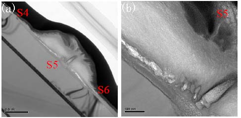
Figure 2437 shows an example of C, O, and Si contaminated bond pads. Area S6 had an abnormal film on the native Al oxide, while area S5 presented nonhomogeneous, loose and empty SixAlyCzOm materials in the hemispherical defect.  These pad defects existed only at wafer edge because backside grinding was the root cause of the contamination.

Contaminated bond pads

Figure 2437. Contaminated bond pads. Adapted from [2]


[1] Y. N. Hua, S. Redkar, C. K. Lau, “A Study on Non- Stick Aluminium Bondpads due to Fluorine Contamination using SEM, EDX, TEM, IC, Auger, XPS and TOF-SIMS Techniques,” Proceedings from the 28th International Symposium for Testing and Failure Analysis, Phoenix, Arizona, November, 2002, pp. 495-504.
[2] Paul Yu, Jamie Su, Qiang Gao, Ming Li, Chorng Niou, Study of Aluminum Pad Contamination Sources during Wafer Fabrication, Shipping, Storage and Assembly, International Symposium on High Density packaging and Microsystem Integration, 2007. HDP '07.


=================================================================================

The book author (Yougui Liao) welcomes your comments, suggestions, and corrections, please click here for submission. If you let book author know once you have cited this book, the brief information of your publication will appear on the “Times Cited” page.