Chapter/Index: Introduction | A | B | C | D | E | F | G | H | I | J | K | L | M | N | O | P | Q | R | S | T | U | V | W | X | Y | Z | Appendix
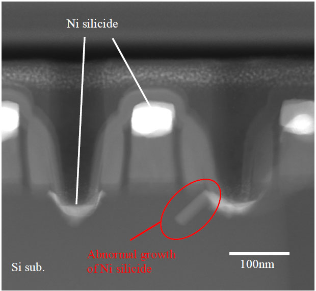
| The cross-sectional STEM image of a MOS transistor in Figure 2443 presents nickel silicide penetration into junction due to the abnormal growth of the Ni silicide. This Ni silicide penetration induced junction leakage-current in the MOS transistor. With plasmon loss in EELS, Kudo et al. [1] suggested that the Ni silicide in the abnormal growth area was nickel-disilicide (NiSi2). Starting from the understanding of the various mechanisms of crystalline growth, the abnormal growth can suppressed by controlling the crystal microstructure of the Si substrate, for instance, by using Si ion implantation [2], nitrogen ion implantation [3], the optimization of the conditions of gate sidewall etching [1], or the choice of the substrate direction [4].
Figure 2443. Nickel silicide penetration into junction of a MOS transistor due to the abnormal growth of the Ni silicide. [1]
[1] S. Kudo, Y. Hirose, N. Hashikawa, T. Yamaguchi, K. Kashihara, K. Maekawa, K. Asai, N. Murata, K. Asayama and E. Murakami, Analysis of Ni Silicide Abnormal Growth Mechanism Using Advanced TEM Techniques, IEEE International Reliability Physics Symposium, 2008. IRPS (2008) 10074334.
|