Chapter/Index: Introduction | A | B | C | D | E | F | G | H | I | J | K | L | M | N | O | P | Q | R | S | T | U | V | W | X | Y | Z | Appendix
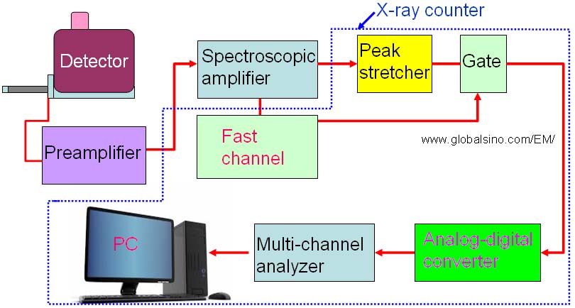
| The schematic in Figure 2526 illustrates the components of an entire EDS system.
Figure 2526. Schematic illustration of the components of an entire EDS system.
Overall, each absorbed X-ray photon generates a charge cloud that is composed of a number of electron-and-hole pairs, and the charge carriers are moved due to high voltage and are collected in the detector. The charge-sensitive preamplifier (PA) converts the charge pairs into a voltage pulse. The pulse is amplified and shaped in a spectroscopic amplifier (SPA). In this SPA process, one needs to optimize some constants such as gain, shaping time, pole zero, and base-line. The maximum of the intensified pulse is detected or stretched by peak-detector or peak-stretcher (PS). Finally, each pulse is individually measured with an analog-digital converter (ADC).
|