
Chapter/Index: Introduction | A | B | C | D | E | F | G | H | I | J | K | L | M | N | O | P | Q | R | S | T | U | V | W | X | Y | Z | Appendix
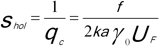
| In off-axis electron holography, the best resolution, and thus the highest spatial frequency qmax can be reconstructed from the sideband and is given by the spacing shol = 1/qc of the interference fringes, [1] given by, The biprism voltage UF is the only variant in Equation 2556a. From the resolution point of view, the biprism voltage UF should be set to as low as possible. On the other hand, the width W of the hologram can be given by, [1] However, in practice, the width W of the hologram is limited by the coherent current of the electron beam and by the strength of excitation of the subsequent intermediate lens. [1] The biprism voltage is provided by a highly stabilized DC power supply (e.g. rel. 10-5) with output voltages of 70 - 300 V for 200 keV incident electrons and 1000 V for 300 keV incident electrons, respectively. [1,3] Zheng et al. [3] set the biprism voltage in their 200 keV microscope in the range of 70 – 80 V, resulting in an overlapping width (W) of interference fringes from 2.5 µm to 3 µm.
[1] Michael Lehmann, and Hannes Lichte, Tutorial on Off-Axis Electron Holography, Microsc. Microanal. 8, 447–466, 2002.
|
 --------------------------- [2556a]
 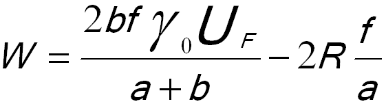 ----------------------- [2557b]