Dependence of BF/ADF-STEM Intensity on Specimen Thickness
- Practical Electron Microscopy and Database -
- An Online Book -

http://www.globalsino.com/EM/  


=================================================================================

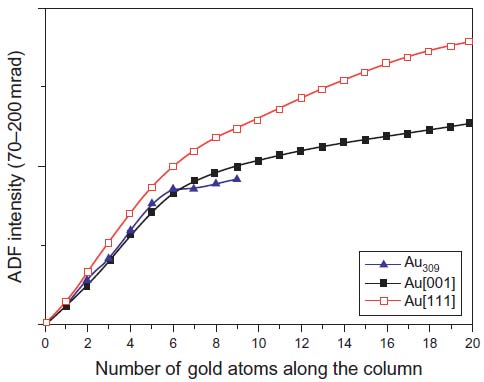
The intensity recorded by ADF STEM detector can be given by, [5]
                intensity recorded by ADF STEM detector -------------------- [2575a]
where,               
         c - a constant,             
         t -- the sample thickness,       
         Zeff -- the effective atomic number of the material,
         ε -- an exponent in the range of 1.6 to 2.0.

In Figure 2575a, multislice simulation presents the total cross section of Au (gold) as a function of the number of atoms in a Au column.[1] In other words, the HAADF intensity depends on the atomic number (Z-contrast) as well as the number of atoms in the column. Without the need for a calibration standard, LeBeau et al. [2] were able to quantify the number and location of the atoms in the specimen from 4 to 33 atom column height when the experimental images taken from a wedge-shaped Au thin foil was compared directly with theory.

HAADF intensity as a function of the  number of atoms along the Au column, obtained by multislice simulation

Figure 2575a. HAADF intensity as a function of the number of atoms along the Au column, obtained by multislice simulation. [1]

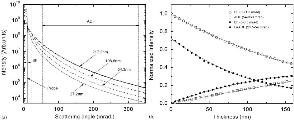
Mkhoyan et al. [3] applied multislice method to simulate the angular distribution of scattered electrons at different thicknesses of amorphous Si specimens in STEM imaging.  Under the optics conditions described in Figure 2575b, only ~60% of the original beam reachs the BF (bright-field) or EELS detector after passing through 100 nm (marked by the red line) of an a-Si specimen if a 21.5-mrad collection aperture is used, and only ~30% if an 8.5-mrad collection aperture is applied. Note that in EELS mode, the collection aperture normally refers to, for instance, the entrance aperture of GIF detector.

Simulated electron scattering in STEM after passing through a-Si at different thicknesses

Figure 2575b. Simulated electron scattering in STEM after passing through a-Si specimens at different thicknesses: (a) Angular distribution of the scattered electrons; (b) Fraction of the scattered electrons of the incident beam into BF/EELS and ADF (annular dark field) detectors. The inner and outer angles of the ADF detector are indicated. Optics conditions are: STEM convergence angle = 10 mrad, Cs = 1.3 mm, and Δf  = 85 nm. Adapted from [3]

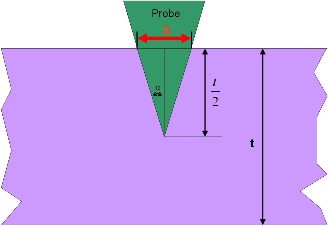
Furthermore, the "local" STEM intensity depends on its spatial resolution. However, the spatial resolution of the measurements in STEM mode can be estimated by the diameter of the probe irradiation on the specimen. Assuming the thickness of the specimen is t, then the spatial resolution is given by (see Figure 2575c):
          Spatial Resolution due to Specimen Drift -------------------------------- [2575b]
where,
          α -- The convergence semiangle.

Diameter of the probe irradiation with specimen thickness t

Figure 2575c. Diameter of the probe irradiation with specimen thickness t.

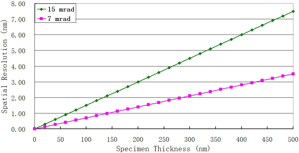
For instance, Figure 2575d shows the spatial resolutions at convergence semiangles 7 and 15 mrad, respectively, based on Equation 2575. Note that such convergence semiangles are used in many TEM systems.

Examples of drift effect on spatial resolution
Figure 2575d. Spatial resolutions at convergence semiangles 7 and 15 mrad, respectively, based on Equation 2575.

Mass-thickness measurement with the scattering contrast method in STEM mode, for a thin amorphous specimen, a small collection semiangle improves the measurement sensitivity, whereas for polycrystalline or single-crystal specimens, a large collection semiangle should be used to reduce diffraction-contrast effects. [4]


[1] Jiang J. Structural characterization and investigation of the growth mechanism for the pentacle nanowires. PhD Thesis, Tsinghua University, 2009.
[2] LeBeau JM, Findlay SD, Allen LJ, Stemmer S. Nano Lett 2010;10:4405–8.
[3] K.A. Mkhoyan, T. Babinec, S.E. Maccagnano, E.J. Kirkland, and J. Silcox, Separation of bulk and surface-losses in low-loss EELS
measurements in STEM, Ultramicroscopy 107 (2007) 345–355.
[4] Huai-Ruo Zhang, Ray F. Egerton and Marek Malac, Local thickness measurement through scattering contrast and electron energy-loss spectroscopy, Micron 43 (2012) 8–15.
[5] T. Walther, Y. Qiu and A. G. Cullis, Measuring the contrast in annular dark field STEM images as a function of camera length, Journal of Physics: Conference Series 241 (2010) 012068.


=================================================================================