Practical Electron Microscopy and Database

An Online Book, Second Edition by Dr. Yougui Liao (2006)

Practical Electron Microscopy and Database - An Online Book

Chapter/Index: Introduction | A | B | C | D | E | F | G | H | I | J | K | L | M | N | O | P | Q | R | S | T | U | V | W | X | Y | Z | Appendix

Nanoprobing Technique for IC Failure Analysis

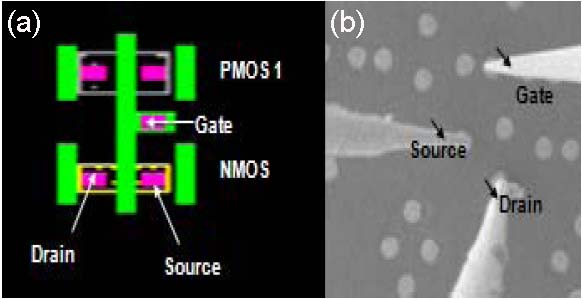
SEM (scanning electron microscopy)-based nanoprobing technique [1] is frequently used to identify the soft failure and non visible defects. Nanoprobing techniques, such as electron beam induced current (EBIC), can offer two-dimensional data; however, they are limited in effectively visualizing junction health in three dimensions. This technique provides the capability of operating probe tips in nanometer range to land exactly on top of the individual source, drain and gate tungsten contact, for instance, as shown in Figure 2825a. The SEM provides a high-resolution real-time image that facilitates locating the failing device and placing the probe tips. In this way, the locations of soft failure and non visible defects can become visible during electrical stressing.

Nanoprobing Technique for IC Failure Analysis

Figure 2825a. (a) Inverter image, and (b) A SEM image showing three tungsten probes (black arrow) landing on tungsten contacts of the NMOS transistor in the inverter. Adapted from [2]

One of the primary challenges in SEM imaging during nanoprobing arises from the need to protect sensitive samples by using low-energy electron beams (low eV), low beam currents, and minimal beam doses. These conditions are essential to prevent damage to the sample, but they significantly affect imaging quality. Specifically, they lead to high noise, low contrast, and image distortions, which complicate the accurate detection and positioning of nanoprobing tips. As a result, ensuring precise and reliable nanoprobing under these conditions requires advanced imaging techniques, careful optimization of SEM parameters and/or more advanced techniques.

AI-driven models can be used to enhance the accuracy and efficiency of SEM imaging during nanoprobing by compensating for the challenges caused by the low-energy imaging conditions with the steps below [3]:

  • Mask R-CNN (Two-stage model): This is a popular neural network for image segmentation and object detection. In nanoprobing, it can be used to detect and accurately localize the probe tips within noisy SEM images. The "two-stage" aspect refers to its method of first proposing regions of interest (RoI) and then refining these regions to precisely segment and classify objects (in this case, the tips).
  • RTMDet + RTMPose (Composition model): These are modern, real-time object detection and pose estimation models. The combination of RTMDet for object detection and RTMPose for determining the orientation (pose) of the probe tips allows for more precise and fast identification of the tips, even when they appear at different angles or positions in the SEM images.
  • YOLOv8 (Single-stage model): YOLO (You Only Look Once) is a real-time object detection model that processes the image in a single pass, making it faster than two-stage models like Mask R-CNN. YOLOv8 is a more advanced version that can quickly identify the tips within an SEM image, balancing speed and accuracy. The "single-stage" aspect means that the model directly predicts the locations and classes of objects without a separate region proposal stage.

750 images were used to train these models, with 600 images generated automatically and 150 from real application scenarios. [3] By training these AI models with a diverse set of SEM images, they can learn to recognize and correctly position the probe tips even in challenging, noisy, and distorted imaging conditions.

Figure 2825b shows four probe tips making contact with the source, drain, gate, and well of a single transistor. This configuration is part of a nanoprobing technique used for electrical characterization during failure analysis. The purpose of this setup is to collect a family of I/V (current-voltage) curves from both the good and failing transistors. Through comparison with a reference, the test revealed a 50 kOhm short between the source and drain of the suspect transistor. This result was consistent with other findings from Scanning Capacitance Microscopy (SCM) that indicated a source-to-drain short in the transistor​.

Four probe tips touch down on the source, drain, gate, and the well of a single transistor

Figure 2825b. Four probe tips touch down on the source, drain, gate, and the well of a single transistor. [4]


[1] D. Faure, C.A. Waggoner, “A New Sub-micron Probing Technique for Failure Analysis in Integrated Circuits”, ESREF 2002.
[2] Ravikumar V K, Ho M Y, Goruganthu R R, Phoa S L, Narang V, Chin J M, Combining High Resolution Pulsed TIVA and Nanoprobing Techniques to identify Drive Strength issues in Mixed Signal Circuits, 2010 17th IEEE International Symposium on the Physical and Failure Analysis of Integrated Circuits (IPFA). 
[3] David Kleindiek, Enhancing Semiconductor Nanoprobing procedures with AI-Driven Tip Detection, ISTFA 2024.
[4] Larry Liu, Yuguo Wang, Hal Edwards, David Sekel, Dan Corum, Combination of SCM/SSRM Analysis and Nanoprobing Technique for Soft Single Bit Failure Analysis, Proc. 30th International Symposium for Testing and Failure Analysis, Worcester, 2004.