|
|
Built-in Electric Field/Potential at
Material Surface due to Electron Irradiation
- Practical Electron Microscopy and Database -
- An Online Book -
|
|
https://www.globalsino.com/EM/
|
|
This book (Practical Electron Microscopy and Database) is a reference for TEM and SEM students, operators, engineers, technicians, managers, and researchers.
|
=================================================================================
Based on the dependence of interaction volume and maximum escape depth on PE (primary electron) beam energy, there are three different cases regarding SE emissions: i) RL ≤ 5λ, ii) RM > 5λ, and iii) RH >> 5λ as shown in Figure 4464 (R is maximum interaction volume and λ is maximum escape depth). For the case of R ≤ 5λ, the two positive and negative charge areas are very close. For the cases of R > 5λ and R >> 5λ, there are two distinct regions inside the interaction volume: a thin near-surface layer with thickness T ~ 5λ in positive charge Q+, and a negatively charged bulk (Q-) with a thickness of about (R–T). As a result, the implanted charge is ΔQ = Q+ + Q-, and the built-in electric field (Ebi) governed by ΔQ is established.
Higher charge density induces higher Ebi values, and vice versa.
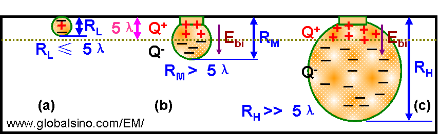
Figure 4464. Schematics of the charge distribution and built-in electric field
inside the interaction volume depending on maximum PE range (R).
This electric field can modify and can also be modified by the processes of the generation and the escape probability of SEs, as well as of the trapping and detrapping of the PEs.
|
=================================================================================
The book author (Yougui Liao) welcomes your comments, suggestions, and corrections, please click here for submission. If you let book author know once you have cited this book, the brief information of your publication will appear on the “Times Cited” page.
|
|