Chapter/Index: Introduction | A | B | C | D | E | F | G | H | I | J | K | L | M | N | O | P | Q | R | S | T | U | V | W | X | Y | Z | Appendix
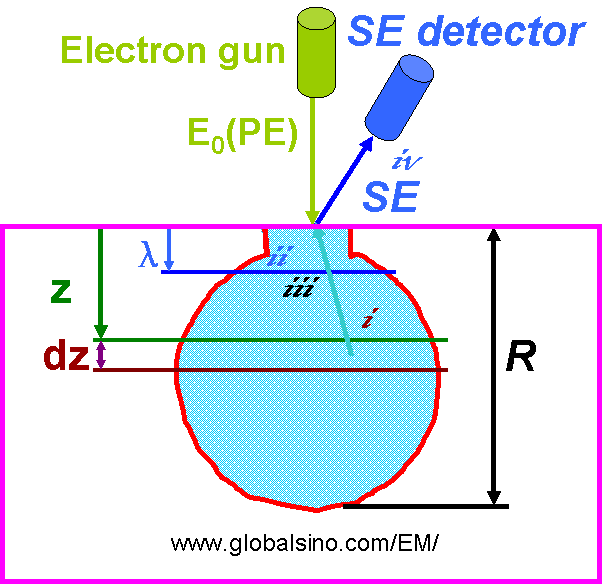
| There are mainly four processes which determine secondary electron (SE) emission from a material surface: Processes i), ii) and iv) strongly depend on the properties of the materials, while process iii) mostly depends on surface properties as shown in Figure 4473.
Figure 4473. Schematic representation of four main processes which determine SE emission. SE imaging: Reimer [3] summarized the process of contrast generation in SE images. In SE imaging, process iv) does not contribute to SE imaging signal. However, there is other factor, which controls the SE imaging signal: v) The emitted SEs are accelerated in vacuum so that a fraction of SEs reachs the electron detector, characterized by D. Therefore, the SE signal is a product of these four factors, given by, S = G·T·P·D ----------------------------- [4473a] Assuming D is equal to 1, the SE yield is given by, S = G·T·P = S/I0 --------------------------- [4473b] where, Note that the escape probability P depends strongly on the depth z where the SE is generated, and becomes small for SEs generated below the escape depth.
[1] Joy DC (1987) J Microsc 147(1):51.
|