| One important issue of EM specimen preparation using FIB is known as the curtaining effect. Materials with different milling behavior above the region of interest result in different sample thicknesses below. Such milling artifact can make detailed analysis of the structures difficult or even
impossible. The FIB-curtained surfaces appear:
i) Milled faces show lines (more or less materials were removed).
ii) Irregular non-flat surface (may obscure features).
Curtaining is created by spatial variation of the sputter rate of the specimen and the modulation of the current density by forward scattering of the ions. This effect presents the formation of striations across the milling face when the sample has:
i) A surface with uneven topography and structures (e.g. rough surface) [1 - 2] (see Figure 4502a). These shadowing effects on topology during cross-sectioning are prevalent.
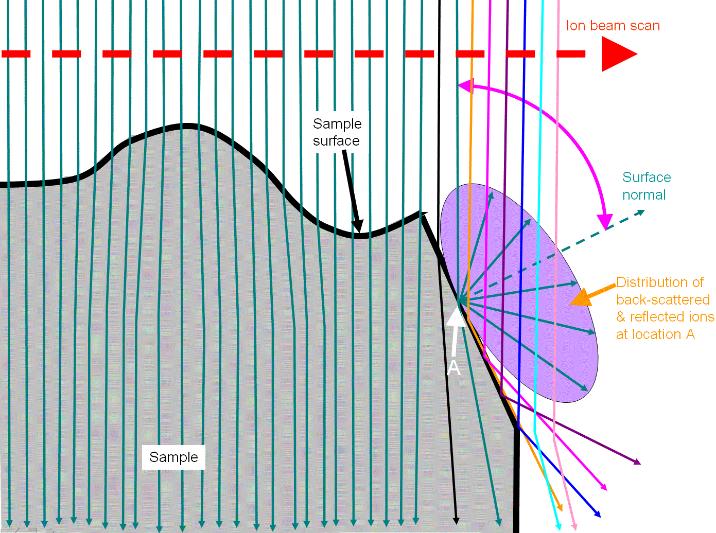
Figure 4502a. Milling behavior due to the roughness of the specimen surface. Topography and tilted surface of the specimen induce deflection of incident ion beam, and thus the local ion dose and local milling speed are modulated. All these factors determine the shape and roughness of the finally milled face. |
ii) A surface with uneven chemical composition [1 - 2].
iii) Composites of hard and soft materials. For instance, the difference in FIB milling rates of various materials in a semicoductor device can cause such curtaining when milling cross-sections.
iv) Height steps (e.g. patterned structures in semiconductors)
v) A porous structure.
vi) Curtaining effect increases with lower acceleration voltages which is used for high quality samples.
This effect often gives trouble to the microelectronics industry because the device structures exist at wafer surfaces. The curtaining artifact occurs when the FIB-sputtering rates are different at different locations (e.g. a tungsten contact to silicon [4]) or voids presents within the specimen.
An immediate consequence of the curtain effect related to TEM specimen is:
i) The specimen will no longer have a uniform thickness.
ii) The specimen will be bad for quantitative image analysis.
To eliminate the curtaining artifacts, one can use hardware- and/or software-based solution [11]:
i) Avoid the curtaining effect by making sure that the ion beam meets only homogeneous material:
i.a) Remove all material with different sputtering behavior before starting the FIB steps [9];
i.b) Change the geometry in a way that the ion beam comes from a homogeneous direction [10], e.g. from the homogeneous sides or bottom [1, 3, 5, 6].
ii) Use thick, uniform and dense protection cap;
iii) Rock stage. Figure 4502b shows that these typical curtaining effects on Si substrate and TSV itself are effectively suppressed by rocking the sample during FIB milling process. In this process, the milling was processed in a sequence of angles without time-consuming low current polishing.
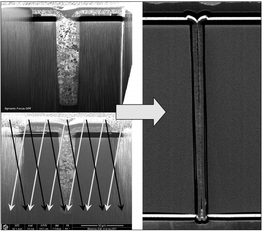
Figure 4502b. Upper left: Curtaining artifacts; Lower left: Milling in a sequence of alternating angles due to rocking the sample; Right: No curtaining effect after rocking the sample. [7] |
iv) Infiltrate the samples, which have porous structures, with low viscosity resin.
On the other hand, obtaining high quality thin TEM-specimen, free from damage, requires low-kV milling. However, the curtaining artifacts can be worse at low kV if it occurs.
[1] Langford RM. 2006. Focused ion beams techniques for nanomaterials characterization. Microsc Res Tech 69:538–549.
[2] Ishitani T, Umemura K, Ohnishi T, Yaguchi T, Kamino T. 2004.
Improvements in performance of focused ion beam cross sectioning:
aspects of ion-sample interaction. J Electron Microsc 53:443–449.
[3] Wang Z, Kato T, Hirayama T, Kato N, Sasaki K, Saka H. 2005. Surface damage induced by focused-ion-beam milling in a Si/Si p-n junction cross-sectional specimen. Appl Surf Sci 241:80–86.
[4] Introduction to Focused Ion Beams, eds. L.A. Giannuzzi and F.A. Stevie, Springer (2005).
[5] Eduardo Montoya et al. Microscopy Research and Technique 6 (2007) 70
1060.
[6] Stephen M. Schwarz1 et al., Microsc. Microanal. 9 (Suppl. 2) (2003) 116.
[7] Maaike M. V. Taklo, Armin Klumpp, Peter Ramm, Laurens Kwakman and German Franz, Bonding and TSV in 3D IC Integration: Physical Analysis with a Plasma FIB, MICROSCOPY AND ANALYSIS, 9, November 2011.
[8] U. Muehle, S. Jansen, L.Hillmann, H.-J. Engelmann and D. Rafaja, FIB-based target preparations of complex material systems for advanced TEM investigations, 1704-1716, in Microscopy: Science, Technology,
Applications and Education, Edited by A. Méndez-Vilas and J. Díaz, Vol. 3, Spain.
[9] Huebner, R., Engelmann, H.-J., Zschech, E.; Effect of TEM sample preparation on quantitative EDXS analysis of SiGe structures;
submitted to Appl.Phys. Lett.
[10] Muehle, U., Sickmann, J., Hillmann, L.; Focused Ion Beam (FIB)-basierte Zielpräparation an Transistoren der 70 nm -
Generation zur Elektronenholographie; Praktische Metallographie 46 (2009): 509-520.
[11] Thomas Henning Loeber, Bert Laegel, and Sandra Wolff, Reducing curtaining effects in FIB/SEM applications by a goniometer stage and an image processing method, Journal of Vacuum Science & Technology B, Nanotechnology and Microelectronics: Materials, Processing, Measurement, and Phenomena 35, 06GK01 (2017); https://doi.org/10.1116/1.4991638.
|
