Chapter/Index: Introduction | A | B | C | D | E | F | G | H | I | J | K | L | M | N | O | P | Q | R | S | T | U | V | W | X | Y | Z | Appendix
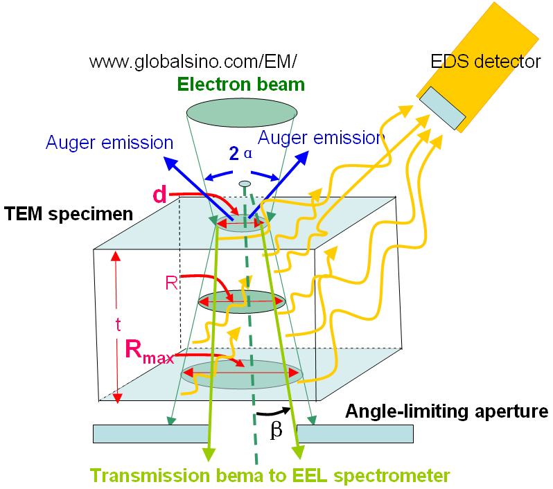
| Spatial resolution is a quite general concept and is a very critical parameter in EDS microanalysis. Since the spatial resolution is determined by the interaction between the electron beam and specimen, it is a function of the incident electron beam size (d) defined as the Full-Width Half-Maximum (FWHM) of the Gaussian electron intensity and the beam broadening (b) that is caused by elastic scattering of the electrons within the interaction volume in the specimen. If the beam retains a Gaussian distribution in the interaction volume, the spatial resolution can be roughly given by, Figure 4629 shows the schematic illustration of the broadening of electron beam within a thin specimen and of generations of EDS, EELS and AES signals. This beam broadening affects the spatial resolution of EDS significantly, but does not affect those of EELS and AES too much. d, R and Rmax are the spot size , the average diameter, and the maximum diameter of the electron beam within the specimen, respecitively. For instance, when an incident electron beam at an accelerating voltage of 20 kV irradiates a copper (Cu) material, the generation depth and width of X-rays are ~ 1.5 µm and ~ 1 µm, respectively. The generation width determines the spatial resolution of X-ray based measurements, e.g. EDS.
Figure 4629. Schematic illustration of the broadening of electron beam Based on the beam spreading theory, to improve the EDS spatial resolution, one need to use as thin a specimen, as small a probe diameter and as high an accelerating voltage as possible. In general, the spatial resolutions of EDS measurements are about 1 µm for SEM and between 1 and 20 nm for TEM (103 times better than SEM/EPMA(Electron Probe Micro-Analysis)). It should be pointed out that a spatial resolution of ~2 nm is attainable on analytical (S)TEMs with an FEG, while with a LaB6 gun, the equivalent value is ~10 nm. For SEM-EDS measurements on bulk materials, very high accelerating voltages decrease spatial resolution. Therefore, for low-energy EDS measurements of heavy elements in bulk materials, the spatial resolution can be enhanced if the X-ray lines of a proper low-excitation energy are used. With an accelerating voltage of 5 kV, the K line is available only for atomic numbers below 20, above which L lines is needed, and M lines must be used for atomic numbers above 42. Note that the bremsstrahlung background forms a smooth continuum with count rate per unit energy interval that is independent of detector resolution, while the peak height of characteristic X-rays is inversely proportional to resolution.
|