| In SEM (secondary electron microscopy) observations, especially for electrically isolated structures, charging mechanisms originate from competition between the injection of primary electrons (PEs) into the specimen (contributing to negative charging) and the emission of secondary electrons (SEs) from the specimen (contributing to positive charging). During electron interaction with the specimen, self-regulation processes take place leading to changes in the SE yield δ from its initial value (δ0), to a steady-state value (δC∞). δ0 represents the SE yield obtained from short-pulse of electron beam to prevent charging and δC is the SE yield obtained under permanent irradiation, and the subscript ∞ represents the steady state under charged condition.
For SEM measurements, the charge conservation principle can give,
I0 = I0(δ+η) + dQ/dt + Iout --------------------- [4848]
where,
dQ/dt -- the increase of charge into the specimen,
I0 -- The incident beam intensity,
Iout -- the intensity escaping from the specimen.
When the evacuation of charges to ground is negligible, the steady state for the SE yield (δ) corresponds to the ratio of number of electrons emitted into the vacuum and number of electrons injected into the specimen, meaning that the SE current minus the primary electron current determines the charging state of the specimen. η is the yield of backscattered electrons. Figure 4848a shows the schematic illustration of the sum, δ+η, in thick TEM or bulk samples as a function of the
accelerating voltage of primary electrons (VPE). (δ+η)mp represents the maximum sum of δ+η at the most probable energy (MPE) of SE emission and backscattering (Vmp). Vcr1 and Vcr2 are two critical voltages at which δ is equal to 1, namely the total charge conservation leads to a steady state given by δC∞ + ηC∞ = 1. Note that, typically, Vcr1 is < 100 eV and Vcr2 about 2 kV for insulators [1].
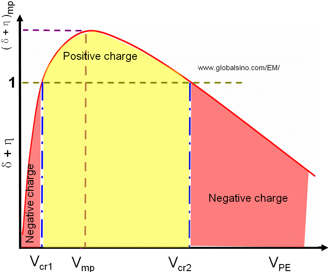
| Figure 4848a. Schematic illustration of the sum δ+η, in thick TEM or bulk samples, as a function of the
accelerating voltage of primary electrons (VPE). Vcr2 is normally between 2-4 keV. In the voltage range of incident electron beam in yellow, the low positive charging is few volts. The voltage (Vmp) of the incident beam at the maximum sum (δ+η)mp is in the range of 400-800 eV. The voltage range in orange shows negative charges, while that in yellow shows positive charge. |
In Figure 4848a, the two blue dotted lines show the two accelerating voltages of the primary electrons at which the electrically isolated structure is not charged at all during imaging. Therefore, the reason why the specimen needs to be grounded for high quality SEM imaging is that we cannot practically have such exact accelerating voltages for a “neutral” condition. The light yellow area shows the structure is positively charged at a few volts to medium voltages because δ+η > 1, while the light red areas show that it is negatively charged at low and high voltages. Both LVSEM and CCVC pattern of e-beam testing work in the light yellow region with weak positive charging to avoid strong negative charging at high accelerating voltages. Low-voltage SEMs are increasingly applied to avoid negative charging, but positive charging effects may still cause disturbance.
When the incident electron beam irradiates on a homogeneous flat insulating surface, the charge distribution in the materials is not invariant over the interaction volume. The surface is charged positively, while the interraction volume has different charge distribution. Due to the incident electrons in excess, there is a negative charge distribution of relative weight 1−η generated down to the maximum penetration depth of the incident beam, spreading over a more or less spherical volume of approximate diameter R. In letaral directions, the charges are nonuniform.
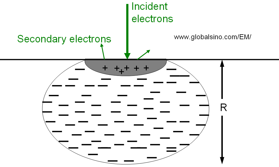
| Figure 4848b. Charge distribution due to the irradiation of an incident electron beam. The surface is positively charged due to secondary electron generation, while the "bulk" is charged negatively. |
On the other hand, Figure 4848c shows the schematic illustration of the sum δ+η, in thin TEM samples, as a function of the
accelerating voltage of primary electrons (VPE). The charge in the thin TEM sample is always positive since the voltage of the primary beam is higher than Vcr1 due to ionization through emission of secondary electrons.
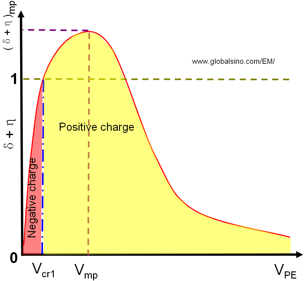
| Figure 4848c. Schematic illustration of the sum δ+η, in thin TEM samples, as a function of the
accelerating voltage of primary electrons (VPE). |
Table 4848a lists the charging properties under the incident electron beams in EMs. For the cases that the charging does not deflect the incident beam, the samples can be observed without coating.
| Table 4848a. Charging properties under incident electron beams in EMs. V is charging voltage. |
| Sample |
Material |
Vcr1 |
Vmp |
(δ+η)mp |
Vcr2 |
V
at < Vcr1 |
V
between
Vcr1 and Vcr2 |
V
at > Vcr2 |
| Surface |
|
|
|
|
|
|
< 10 eV |
|
| Thick TEM and bulk samples |
General |
40 eV |
400 - 800 eV |
|
0.5-4 keV |
|
A few volts to medium voltages |
Low and high voltages |
| Insulators |
< 100 eV |
|
|
2 kV |
|
|
|
| Carbon |
|
|
|
0.65 [6] |
|
|
|
| Acetal |
|
|
|
1.65 keV [9] |
|
|
|
| Al interconnect |
150 eV [3] |
300 eV [3] |
1.2 [3] |
0.7 ~1.05 keV[3, 6] |
|
|
|
| A21470 resist on SiO2 |
|
|
|
0.90 keV [7] |
|
|
| AZ1470 resist on poly-Si |
|
|
|
1.10 keV [7] |
|
|
| Chromium on glass |
|
|
|
2.0 keV [7] |
|
|
| GaAs |
|
|
|
2.6 keV [6] |
|
|
| Glass passivation |
|
|
|
2.0 keV [6] |
|
|
| HPR electron resist |
|
|
|
0.55 keV [6] |
|
|
| Muscovite mica: KAl2(AlSi3O10)(OH)2 |
< 100 eV |
|
|
4.85 keV [4] |
|
|
| PBS electron resist on Cr |
|
|
|
0.70 keV [7] |
|
|
| 5% PBT/95% nylon mixture |
|
|
|
1.40 keV |
|
|
| PVC |
|
|
|
1.65 keV [9] |
|
|
| Si substrate with a 3 nm SiO2 coating |
|
|
|
1.25 keV |
|
|
| Si substrate with a 3 nm C coating |
|
|
|
0.95 keV |
|
|
| Si substrate without coating |
|
|
|
1.15 keV |
|
|
| Al2O3 |
|
|
|
20 keV |
|
|
| KCl |
|
|
|
6 keV |
|
|
| MgO |
|
|
|
3.5 keV |
|
|
| NaCl |
|
|
|
6 keV |
|
|
| SiO2 |
|
|
|
3.0 keV [6] |
|
|
| Sample thickness |
|
|
|
Increases with decreasing thickness |
|
|
| Teflon |
|
|
|
1.82 keV [9] |
|
|
| Effects on incident beam |
|
|
|
|
Does not deflect the incident beam |
Deflect beam |
| Thin TEM samples |
General |
< 100 eV |
|
|
Not applicable |
|
|
|
| Insulators |
< 100 eV |
|
|
|
|
| Effects on incident beam |
|
|
|
|
Does not deflect the incident beam |
| Sample tilt |
|
|
|
|
Increases with increasing tilt angle |
|
|
|
It is necessary to highlight some key fundamentals for Table 4848a:
i) Since few secondary electrons have more than 10 eV of energy, thus the surface could not charge to a positive potential of more than ~ 10 volts.
ii) If an isolated structure in the sample charges negative, then no clear source limits the amplitude of the voltage from the the charging when there is no leakage. Therefore, the maximum voltage can be the incident beam energy.
iii) The positive charging is a self limiting process since this charging causes more SE to be reattracted to the surface. In other words, the positive increase in surface potential is limited because the low-energy secondary electrons cannot overcome an increasing surface potential barrier.
iv) Negative charging is not a self limiting process. Therefore, negative charging is normally more harmful in microelectronic devices.
v) Control of the sign of charging can be easily achieved via the accelerating voltage of the incident electron beam.
vi) Factors affecting the sign and charging rate:
vi.a) Beam energy
vi.b) Sample tilt. Vcr2 increases with increasing tilt angle due to larger backscattered and
secondary electron yields.
vi.c) Scan rate
vii) The highest energy cross over Vcr2 in Figure 4848a provides the most suitable conditions for good working conditions of
electron optics for clear pictures in SEM.
viii) The process is very complicated when the primary electron (PE) range is larger than the maximum escape depth of the SEs.
ix) Electron/hole pairs can be generated by the primary electrons.
Table 4848b. Example of charged structures. |
| Structure |
Voltage from charging |
Measurement technique |
Reference |
Al interconnect, Si mesa in SOI |
+6 ~ 10 V |
e-beam tester with a spectrometer |
[2] |
| > -16 V |
[2] |
The actual charging process of an electrically isolated structure is very complicated and is determined by many factors:
i) The incident electrons interact with the specimen in the manner of many complex and dynamic processes, including scattering, diffusion, mobility, trapping, combination, etc;
ii) The charging process is time-dependent;
iii) The irradiation condition and the internal property of the specimen can affect the charging process;
iv) Adjacent structure can affect the charging process of a location.
The charge accumulation results in:
i) unstable imaging conditions,
ii) loss of resolution due to the defocusing of the primary beam probe.
iii) permanent elemental redistribution due to migration of mobile ions under the influence of the induced electrostatic field in some specimens.
[1] Reimer, L. (1993) Specimen charging and damage. Image Formation in
Low Voltage Scanning Electron Microscopy, Chap. 5, pp. 71 - 135. SPIE
Press, Bellingham.
[2] T. Aton, S. C. J. Garth, J. N. Sackett, and D. F. Spicer, Characteristics of a virtual immersion lens spectrometer for electron beam testing, Journal of Vacuum Science & Technology B 6, 1953 (1988).
[3] T.J. Aton; K.A. Joyner; C.H. Blanton; A.T. Appel; M.G. Harward; M.H. Bennett-Lilley; S.S. Mahant-Shetti, Using scanned electron beams for testing microstructure isolation and continuity, 29th Annual Proceedings Reliability Physics 1991, DOI: 10.1109/RELPHY.1991.146020.
[4] G. Blaise, F. Pesty,a and P. Garoche, The secondary electron emission yield of muscovite mica: Charging kinetics and current density effects, Journal of Applied Physics 105, 034101 (2009).
[5] D. C. Joy, Control of Charging in Low-Voltage SEM, 11, 1-4 (1989).
[6] D. C. Joy, A model for calculating secondary and backscattered
electron yields. J Microsc 147,s 1 (1987).
[7] Frosien J, Lischke B: Micrometrology with electron probes. In
Microcircuit Engineering 1986. (Eds A. Heuberger and H
Beneking). Academic Press, London (1985) 441.
[8] Kraus SJ, Adarns WW, Kumar S, Reilly T, Suziki T: Low
voltage, high resolution SEM of polymers. Proc 45 Ann
Meeting EMSA. (Ed. GW Bailey). San Francisco Press,
San Francisco (1987) 466.
[9] Vaz OW, Krause SJ: Low voltage scanning electron microscopy
of polymers. Proc 44th Ann Meeting EMSA. (Ed. GW
Bailey). San Francisco Press, San Francisco (1986) 676. |
