Chapter/Index: Introduction | A | B | C | D | E | F | G | H | I | J | K | L | M | N | O | P | Q | R | S | T | U | V | W | X | Y | Z | Appendix
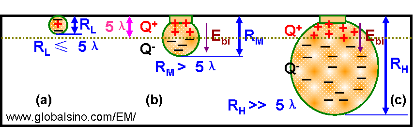
| In SEM (secondary electron microscopy) observations, especially for thick insulators, charging mechanisms originate from competition between the trapping of primary electrons (PEs) injected into the specimen or generated secondary electrons (SEs) (contributing to negative charging) and the emission of secondary electrons (SEs) from the specimen (contributing to positive charging). Based on the dependence of interaction volume and maximum escape depth on PE (primary electron) beam energy, there are three different cases regarding SE emissions: i) RL ≤ 5λ, ii) RM > 5λ, and iii) RH >> 5λ as shown in Figure 4566 (R is maximum interaction volume and λ is maximum escape depth). For the case of R ≤ 5λ, the two positive and negative charge areas are very close. For the cases of R > 5λ and R >> 5λ, there are two distinct regions inside the interaction volume: a thin near-surface layer with thickness T ~ 5λ in positive charge Q+, and a negatively charged bulk (Q-) with a thickness of about (R–T). As a result, the implanted charge is ΔQ = Q+ + Q-, and the built-in electric field (Ebi) governed by ΔQ is established.
The actual charging process of an electrically isolated structure is very complicated and is determined by many factors:
|