Chapter/Index: Introduction | A | B | C | D | E | F | G | H | I | J | K | L | M | N | O | P | Q | R | S | T | U | V | W | X | Y | Z | Appendix
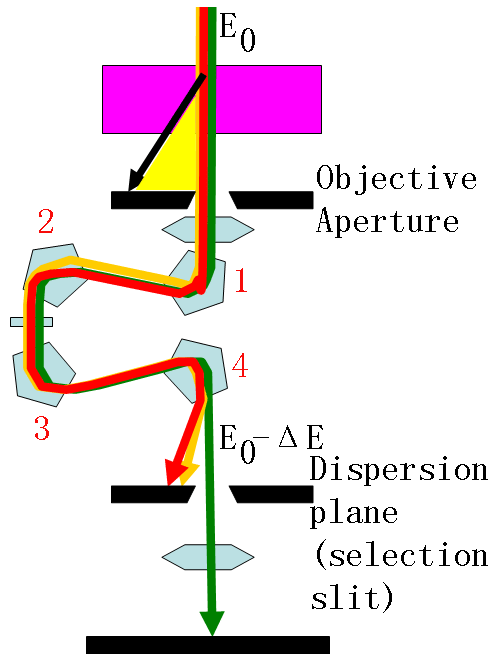
| Energy dispersion can normally be calibrated using a drift tube in the magnetic sector. As an example, Figure 4890a shows the schematic of dispersion plane in Omega filter. A limitation of the magnetic prism-based EELS detection system is the spectrum drift in the energy dispersion direction. An example of energy dispersions of omega-filters is 0.85 µmeV−1 at 300 kV. [1]
In order to record the detailed fine structure of the edges, core-loss edges should be recorded with a small dispersion, e.g. 0.1 or 0.05 eV per channel.
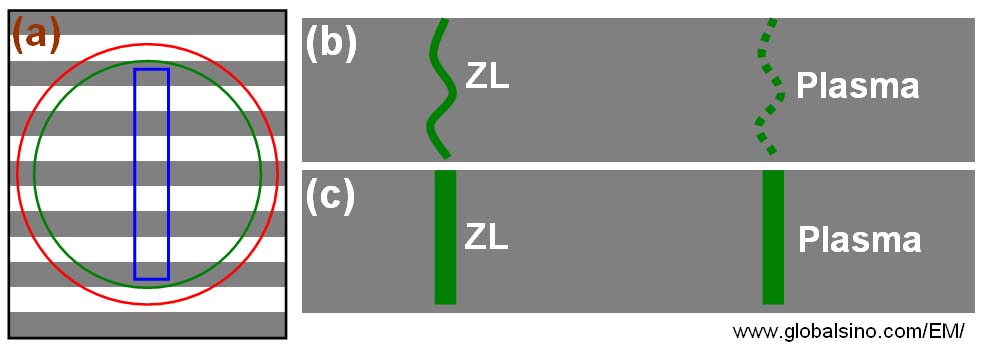
The setting of the energy dispersion in EELS measurements can be changed depending on the intensity of the signal. For instance, the signal of Si-K edge is about two orders of magnitude weaker than that of the L2,3 edges so that the energy dispersion for Si-K edges is 0.30 eV, while 0.051 eV for Si-L2,3 edge per pixel (See page3441). Figure 4890b shows the schematic illustration of laterally resolved EELS across the multi-layers in the specimen. The horizontal stripes in Figure 4890b (a) represent the multi-layers in the TEM specimen. At high dispersion (a low eV/channel value), the curvature of the zero loss (ZL) peak on the CCD indicates the non-isochromaticity of the filter, while at low dispersion the curvature of the ZL is hardly visible.
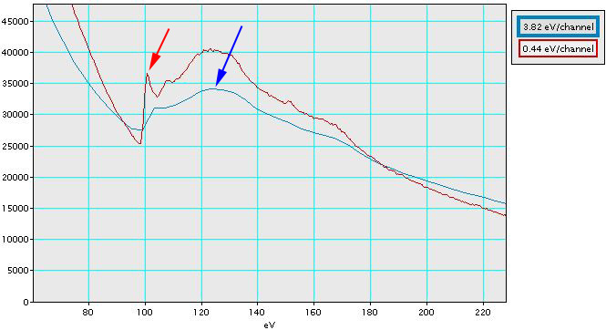
The practical (real) energy resolution of EELS in a TEM depends not only on the energy spread of the electron source, but also on instabilities in accelerating voltage of the electron beam, spectrometer energy dispersion and stray electromagnetic field. As an example of the binning effects on the energy resolution and the background of EEL spectra, the EELS of Si is shown in Figure 4890c. The two spectra were taken at energy dispersions of 0.44 eV/channel and 3.82 eV/channel, respectively. The full-width at half-maximum (FWHM) of the small peak marked by the red arrow is only 2 eV; however, the energy of each channel (pixel) with energy dispersion of 3.82 eV/channel is 3.82 eV. Therefore, such small peak is invisible even though the same EELS system and electron microscope are used for both spectra. Furthermore, the height of the peak marked by the blue arrow is smaller for the greater energy dispersion (3.82 eV/channel).
Note when the energy-loss spectrum is not focused at the energy-selecting slit, normally at low energy-dispersions (high eV/pix values), the shadow of the slit edges in the energy-loss spectrum will not be sharp.
[1] Yoshio Bando, Masanori Mitome, Dmitri Golberg, Yoshizo Kitami, Keiji Kurashima, Toshihiko Kaneyama, Yoshihiro Okura and Mikio Naruse, New 300 kV Energy-Filtering Field Emission Electron Microscope, Jpn. J. Appl. Phys. Vol. 40 (2001) pp. L1193 – L1196.
|