Chapter/Index: Introduction | A | B | C | D | E | F | G | H | I | J | K | L | M | N | O | P | Q | R | S | T | U | V | W | X | Y | Z | Appendix
In EELS systems, the collection angle, β, of electrons leaving the specimen is determined by the spectrometer entrance aperture and camera length. We know that the sizes of the EELS entrance apertures are fixed. Therefore, in principle, it is easy to understand that the transmitted electrons or different diffracted beams can be collected by moving the entrance aperture down or up, as shown in Figure 4936a, which corresponds to the change of the camera length. However, a couple of reasons make the entrance aperture movement impossible, for instance, it is not convenient to mechanically move the entrance aperture, together with the EELS system, up and down in a vacuum condition.
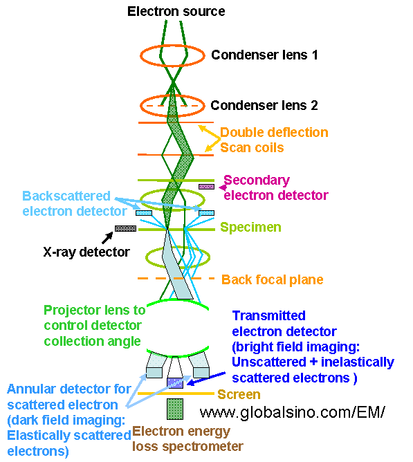
Instead of moving the entrance aperture up and down, we can conveniently change the lens currents to zoom in (magnify) or zoom out (demagnify) the diffraction pattern on the entrance aperture. This zoom-in and zoom-out process are then converted to the correpsonding camera lengths on the commercial microscopes. Therefore, the collection angles of the EELS entrance aperture can be varied simply by changing the effective camera length. Generally speaking, large collection angles of EELS will give high intensity but poor energy resolution. If it is in diffraction mode and the control collection angle (β) is controled by the entrance aperture, then a large aperture (high intensity, high β) will lower the resolution and vice versa. Furthermore, smaller collection angles also give a higher signal-to-noise ratio in the EELS spectrum. The schematics in Figure 4936b shows the electron optical column in a modern analytical electron microscope operated in STEM mode, indicating the projector lens controlling detector collection angle.
Figure 4936b. Schematics of the electron optical column in a modern For thick TEM specimens, e.g. ≥80 nm for Si, the surface-plasmon effects becomes negligible, while the beam spreading becomes significant because more electrons suffer inelastic collision in larger scattering angles. In this case, more electrons scatter outside the finite collection aperture. Table 4936. Examples of collection angles of EELS measurement in different microscope conditions.
The collection angle for an energy loss can simply be optimized to an angle slightly larger than the relevant characteristic inelastic scattering angle (θE), for instance, for 100-keV incident electrons, θE has a value of 1 mrad for a 200 eV energy loss, while 10 mrad for a 2 keV energy loss.
[1] Peter W. Hawkes, Advances in Imaging and Electron Physics: Aberration-corrected Electron Microscopy, Volume 153, 2008.
|