Chapter/Index: Introduction | A | B | C | D | E | F | G | H | I | J | K | L | M | N | O | P | Q | R | S | T | U | V | W | X | Y | Z | Appendix
| The advantages and disadvantages of ExSolve Wafer TEM Prep DualBeam for sample preparation and imaging are:
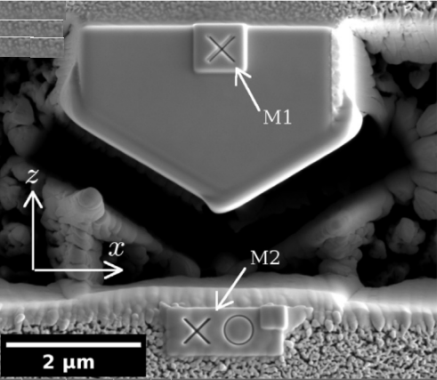
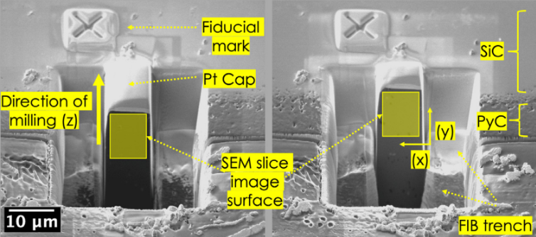
In fiducial markers are used for on-the-fly drift correction during the focused ion beam (FIB) imaging process. These markers help maintain alignment by allowing the system to correct any drift in the ion beam during serial sectioning. Specifically, the top fiducial marker is used for drift correction in FIB images, while other fiducial markers are used for post-milling alignment of scanning electron microscope (SEM) images to ensure accurate 3D reconstruction without distortion. In automated TEM lamella preparation for FIB-SEM tomography, fiducial markers play a crucial role in ensuring precise alignment and tracking of the region of interest (ROI) throughout milling and imaging operations. The top fiducial marker is used for on-the-fly drift correction in FIB images, helping to maintain alignment by allowing the system to correct any drift in the ion beam during serial sectioning. Additional fiducial markers, such as cross and circular markers, assist in post-milling alignment of SEM images, supporting accurate 3D reconstruction without distortion. This setup ensures that the correct region is analyzed consistently, allowing for high-fidelity imaging across multiple milling and imaging steps, as shown in Figure 0016a, where an SEM image displays the top view of the ROI.
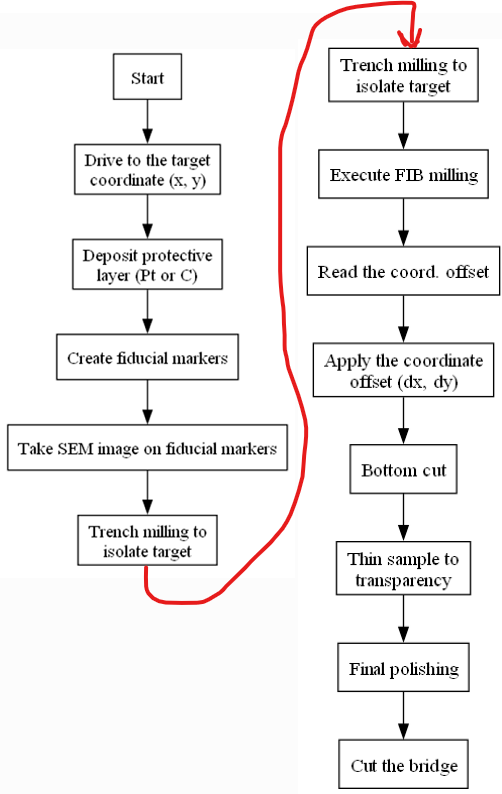
As shown in Figure 0016b, the automated ex situ lift-out process for FIB TEM sample preparation involves a series of organized steps designed to isolate and prepare a sample for transmission electron microscopy (TEM) analysis. The procedure begins with driving the FIB stage to the target coordinate. Then, a protective layer (typically platinum or carbon) is deposited over the area of interest to prevent damage from ion milling. Fiducial markers are then created around the region for precise alignment, followed by capturing an SEM image to verify positioning. Next, initial trench milling is performed to isolate the target sample. A bottom cut then fully detaches the sample. After those milling steps, a coordinate offset is determined and applied to refine the sample's position. The sample then undergoes final thinning and polishing steps to achieve the electron transparency required for TEM imaging. Then, a bridge cut releases the sample for transfer. This automated, structured process ensures high-quality sample preparation with minimal manual intervention, enabling accurate and efficient TEM analysis. Finally, the sample is transferred for ex situ lift-out. The entire preceding procedure before ex situ lift-out can be executed using automated scripts or predefined recipes.
Figure 0016b. Automation script diagram.
[1] Mangipudi, K. R., Radisch, V., Holzer, L., & Volkert, C. A., A FIB-nanotomography method for accurate 3D reconstruction of open nanoporous structures. Ultramicroscopy, 163, 38–47. https://doi.org/10.1016/j.ultramic.2016.01.004, 2016.
|