Chapter/Index: Introduction | A | B | C | D | E | F | G | H | I | J | K | L | M | N | O | P | Q | R | S | T | U | V | W | X | Y | Z | Appendix
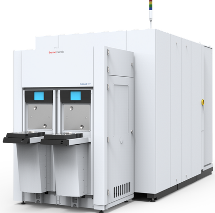
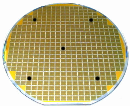
| The ExSolve Wafer TEM Prep DualBeam, TEMLink, and Thermo Fisher Metrios TEM are interconnected tools in the workflow for advanced semiconductor failure analysis and materials characterization, particularly in the preparation and analysis of Transmission Electron Microscopy (TEM) samples. The ExSolve Wafer TEM Prep DualBeam system in Figure 313a is a tool designed for preparing TEM samples directly from full wafers (see Figure 313b) or die. It uses DualBeam technology, which combines a focused ion beam (FIB) and a scanning electron microscope (SEM), to precisely extract and thin down regions of interest on a wafer for TEM analysis. This system is particularly beneficial for semiconductor manufacturing, where precise cross-sectional analysis of materials and devices is required at the nanometer scale. The ExSolve Wafer TEM Prep is optimized for large wafers (e.g., 300mm) and allows automated sample preparation, enhancing throughput and reducing the manual effort typically required in sample preparation for TEM. It is often used to analyze defects, failure mechanisms, and material interfaces in semiconductor devices.
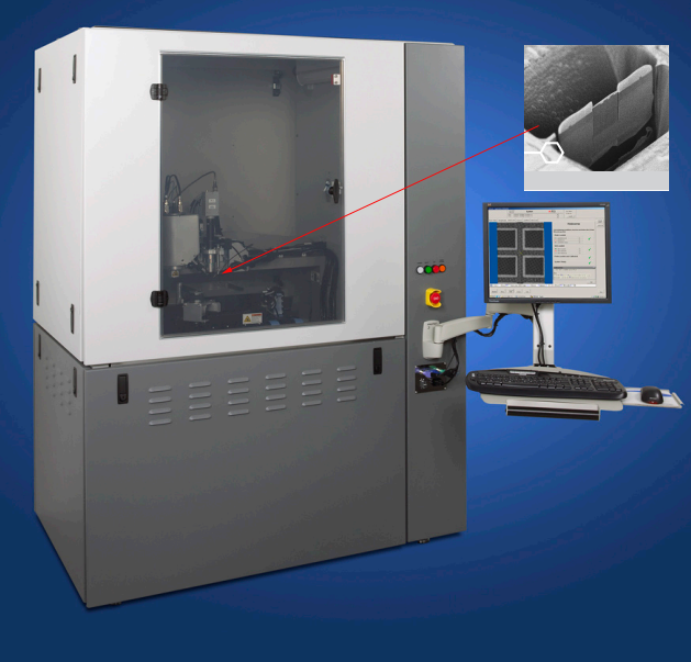
In TEMLink TEM lamella extraction station shown in Figure 313c, the process of picking up a TEM lamella begins with the probe approaching the lamella, which is still attached to the wafer. Using an optical view, the probe can be seen moving toward the lamella from the side. Once the probe is in place, the lamella is carefully detached from the wafer and held at the end of the probe by vacuum suction. The probe then rotates 180° to orient the lamella parallel to the surface of the TEM grid (see Figure 313d). In this position, the lamella is positioned over an opening in the grid. Finally, the vacuum is released, depositing the lamella onto the grid, where it is ready for further transmission electron microscopy (TEM) analysis. This semi-automated process ensures precision and efficiency in lamella handling.
Figure 313d shows an optical image of lift-out sample placed on a carbon coated membrane grid for TEM analysis.
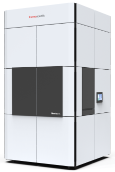
The Thermo Fisher Metrios TEM in Figure 313e is designed primarily for semiconductor applications, offering high-throughput and automated analysis for process control and defect analysis. It provides advanced imaging and analysis capabilities to inspect and measure critical dimensions at the nanometer scale, making it a valuable tool for metrology in the semiconductor manufacturing process.
[1] www.microscop.ru.
|