Chapter/Index: Introduction | A | B | C | D | E | F | G | H | I | J | K | L | M | N | O | P | Q | R | S | T | U | V | W | X | Y | Z | Appendix
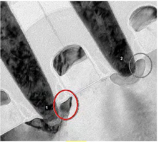
| Larger nickel silicide particles with high resistance are observed at junction leakage. For instance, Figure 1288 shows the larger nickel silicide particle marked by the red circle encroached on the n-LDD (Lightly Doped Drain) region of NMOS transistor, while the smaller nickel silicide particle marked by the grey circle did not cause junction leakage. Note that a larger nickel silicide area represents more consumption of silicon substrate. Therefore, it was proposed that such large nickel silicide particles had phase transformation from NiSi to NiSi2. (NiSi2 has higher resistivity and more consumption, see page2446)
[1] ISTFA 2010: Proceedings of the 36th International Symposium for Testing and Failure Analysis.
|