| This voiding and spiking issue in cobalt silicidation (page2796) is one of the reasons for the transition from cobalt silicide to alternatives like nickel silicide, which is more stable at reduced feature sizes (e.g., 65 nm technology nodes and beyond). Nickel silicide offers advantages like lower resistance, better uniformity, and reduced sensitivity to line width variations, which helps mitigate the voiding and spiking phenomena observed with cobalt silicid.
Nickel silicides (Ni–Si alloys) are applied to reduce the contact resistance between the Si substrates and electrodes in CMOS structures, and to improve gate sheet resistance and poly depletion in gates. The phase diagram of nickel silicides consists of various phases: three polymorphic Ni3Si structures (β1, β2 and β3), Ni31Si12 (γ), NiSi3(D03, D022), Ni5Si2 (D8h), two polymorphic Ni2Si structures (δ = C23, and θ = B82), Ni2Si (C37, D03, D022), Ni3Si2 (ε), NiSi (MnP), NiSi2 (α= CaF2, β), Ni3Si2-ε', NiSi2 (CaCl2 = C35), and NiSi (L10). The schematic diagrams in Figure 2446a show the phase formation in Si—Ni film and silicon crystal/Ni film systems. The indicated temperatures are rough guides for the formation of phases for films a few thousand angstroms thick and an annealing time of 1 hr.
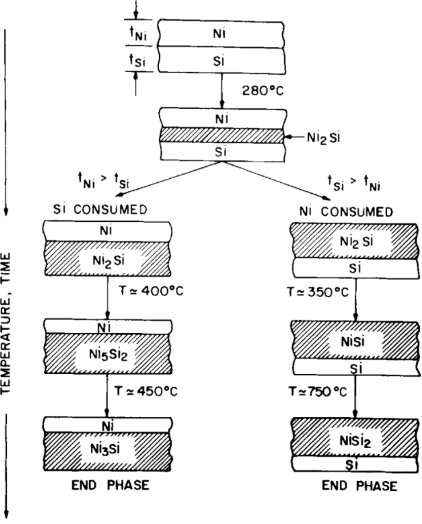
| Figure 2446a. Schematic diagrams indicating the phase formation in Si—Ni film and silicon crystal/Ni film systems. [23] |
Table 2446a lists the lattice constants and formation energies of the most common nickel silicides.
| Table 2446a. Lattice constants (a0, b0, and c0 in Å) and formation energies (E0 in meV/atom) of the most common nickel silicides. |
System |
Name |
a0 (Å) |
b0 (Å) |
c0 (Å) |
E0 (meV/atom) |
Reference |
Ni |
- |
3.519 |
- |
- |
0 |
[8] |
Si |
- |
5.43 |
- |
- |
- |
[8] |
Ni2Si |
δ |
5.009 |
3.732 |
7.066 |
−486 |
[9, 10] |
θ |
3.805 |
- |
4.890 |
−412 |
[11, 12] |
NiSi |
- |
5.177 |
3.325 |
5.616 |
−447 |
[13, 10] |
α |
5.43 |
- |
- |
-327 |
[14, 10, 12] |
NiSi2 |
- |
5.470 |
- |
- |
−347 |
|
Ni3Si |
β1 |
3.506 |
- |
- |
-463 |
[15, 12, 16] |
β2 |
6.972 |
6.254 |
7.656 |
- |
[17] |
β3 |
7.047 |
6.264 |
7.663 |
- |
[17, 18] |
β4 |
5.50 |
6.50 |
4.35 |
−379 |
[19, 12] |
Ni31Si12 |
γ |
6.671 |
- |
12.288 |
- |
[20] |
Ni3Si2 |
ε |
12.229 |
10.805 |
6.924 |
−472 |
[10] |
Figure 2446b shows the differences of the two crystal lattices of NiSi2 and Si. Those differences result in a variety of possible atomic structures at
their interfaces. Such differences in crystal symmetry
lead to the presence of certain defects at
some silicide/Si interfaces. The NiSi2 lattice constant is smaller by ~ 0.4% than that of Si.
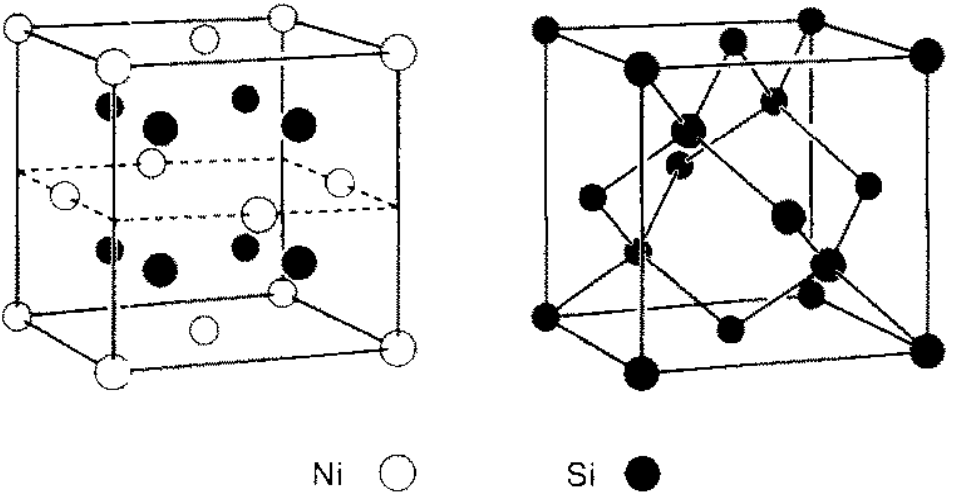
Figure 2446b. Crystal structure of (a) NiSi2 and and (b) Si. [22]
The cross-sectional STEM image of a MOS transistor in Figure 2446c presents nickel silicide penetration into junction due to the abnormal growth of the Ni silicide. The abnormal growth occurred in <110> direction along a {111} plane. This Ni silicide penetration induced junction leakage-current in the MOS transistor. With plasmon loss in EELS, Kudo et al. [1] suggested that the Ni silicide in the abnormal growth area was nickel-disilicide (NiSi2).
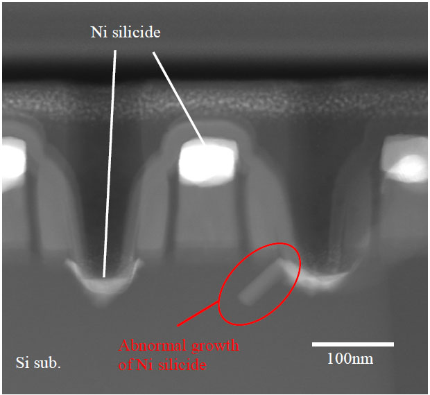
Figure 2446c. Nickel silicide penetration into junction of a MOS transistor due to the abnormal growth of the Ni silicide. [1]
Table 2446b lists the comparison between three types of nickel silicides (Ni2Si/NiSi/NiSi2). The formation of nickel silicides is in the sequence of Ni → Ni2Si → NiSi → NiSi2 with the increase of silicidation temperature. NiSi film is often formed with a two-step silicidation scheme:
i) Chemical dry-clean (CDC) using ammonium fluorosilicate [(NH4)2SiF6] to remove native oxide on Si substrate [5, 6]. This suppresses the formation of high-resistance NiSi2 due to the native oxide on Si [6].
ii) Sputter nickel (Ni) on the Si substrate.
iii) Deposit a titanium nitride cap-film.
iv) Perform an initial annealing (e.g. 300–350°C for 30 s). Ni transforms into dinickel silicide (Ni2Si).
v) Selectively etch non-reacted metal.
vi) Perform a second annealing (e.g. 550–600°C for 30 s). Ni2Si transforms into NiSi [4, 5].
The TEM image in Figure 2446d (a) shows that the high resistance, undulate nickel silicide film that was essentially caused by fluoride contamination. This contamination originated from a chemical dry-cleaning process for silicon (Si) substrate prior to Ni sputtering. The undulate film consisted of thicker NiSi areas (e.g. arrowed by 1) and thinner NiSi2 areas (e.g. arrowed by 2). In Figure 2446d (b), the formation process of the Ni silicide film in different phases was:
i) Fluoride contaminants initially exist in some areas of the Si surface (indicated by the red lines).
ii) Fluoride contaminants impede direct Ni diffusion into Si substrate so that the Ni atoms migrated in the horizontal and then downward directions during the initial silicidation annealing, while direct Ni diffusion into Si substrate occurrs in the clean areas (indicated by the blue arrows).
iii) Vacancies (indicated by the white spots) are formed due to excess Ni diffusion above the contaminants.
iv) During the second (higher temperature) annealing, the vacancies are filled up by excess Si atoms so that the thin Ni2Si areas are transformed into thinner NiSi2, while the thick Ni2Si areas are transformed into thicker NiSi.
Table 2446b. Comparison between Ni2Si, NiSi, and NiSi2.
|
Ni2Si |
NiSi |
NiSi2 |
Note |
Crystal
family |
|
|
|
|
Space group |
Pbnm |
Pnma |
Fm3m |
|
|
21.9 |
20.25 - 20.7 |
19.75 - 20.0 |
Most efficient way to determine phases at nano-scale
|
Ni-L2,3 edge in EELS (eV) |
854 |
855.5 |
857 |
Efficient way to determine phases at nano-scale |
Thin film
resistivity
(μΩ-cm) |
|
14-20 |
40-50 |
|
Sintering
temperature
(°C) |
|
400-600 |
600-800 |
|
| Formation temperature
(°C) |
~200 [21] |
~400 [21] |
~700 [21] |
|
Stable on
Si up to
(°C) |
|
~650 |
|
|
nm of Si
consumed
per nm of
metal |
|
|
3.65 (higher Si consumption) |
|
nm of
resulting
silicide
per nm of
metal |
|
2.34 |
3.63 |
|
Barrier
height to
n-Si (eV) |
|
|
0.66 |
|
Property |
|
Low Si consumption, low thermal budget for
formation, and tolerance for its agglomeration [2, 3] so that it is better for ultrashallow junctions and VLSIs |
|
|
Potential failure in ICs |
|
De-composite into Ni2Si and Si [4] |
|
|
NiSi2 precipitates at dislocations in silicon |
|
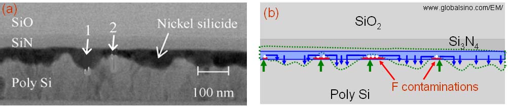
Figure 2446d. Undulate NiSi + NiSi2 film formed due to fluoride contamination: (a) TEM image of nickel silicide film (Adapted from [7]). White arrow "1" points to thicker NiSi, while arrow "2" points to thinner NiSi2. (b) Schematic illustration of the formation process of the structure in (a). The blue box represents the area of the as-deposited Ni film. The area marked by the dotted green curve represents the final nickel silicide as shown in (a). The white spots indicate vacancies that are formed due to Ni out-diffusion during the initial annealing process, while the blue arrows indicate the direction of the Ni out-diffusion. The red lines at the initial interface between the as-deposited Ni and Si substrate represent fluoride (F) contaminants. The green arrows indicate the Si diffusion into the vacancy areas during the second annealing process. |
Figure 2446e shows a HRTEM image used to confirm silicide to be NiSi2.

Figure 2446e. HRTEM image used to confirm silicide to be NiSi2. [24] |
Figure 2446f clearly illustrates poor NiSi formation beneath the contact on the high-resistance side compared to proper NiSi formation at a reference site.
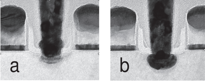
Figure 2446f. XTEM images illustrating poor NiSi formation at the high-resistance site (a) and proper NiSi formation at a reference site (b). [25] |
[1] S. Kudo, Y. Hirose, N. Hashikawa, T. Yamaguchi, K. Kashihara, K. Maekawa, K. Asai, N. Murata, K. Asayama and E. Murakami, Analysis of Ni Silicide Abnormal Growth Mechanism Using Advanced TEM Techniques, IEEE International Reliability Physics Symposium, 2008. IRPS (2008) 10074334.
[2] S. P. Murarka, “Metallization,” in VLSI Technology, 2nd ed., S. M. Sze,
Ed. New York, NY, USA: McGraw-Hill, 1988, ch. 9.
[3] C. Lavoie, C. Detavernier, and P. Besser, “Nickel silicide technology,”
in Silicide Technology for Integrated Circuits, L. J. Chen, Ed. London,
U.K: Instit. Electr. Engineers, 2004, ch. 5.
[4] T. Futase, N. Hashikawa, T. Kamino, T. Fujiwara, Y. Inaba, T. Suzuki,
and H. Yamamoto, “Spike annealing as second rapid thermal annealing
to prevent pure nick silicide from decomposing on a gate,”
IEEE Trans. Semicond. Manuf., vol. 22, no. 4, pp. 475–481, Nov.
2009.
[5] T. Futase, H. Tanimoto, M. Kimoto, H. Tsugane, H. Suzuki, and H.
Tobimatsu, “Removing imperceptible fluoride residue after chemical
dry-cleaning to fabricate uniform low-resistance NiSi film,” J. Vac. Sci.
Technol. B, vol. 29, no. 5, p. 051203, Sep. 2011.
[6] R. Yang, N. Su, P. Bonfanti, J. Nie, and J. Ning, “Advanced in situ
pre-Ni silicide (Siconi) cleaning at 65 nm to resolve defects in NiSix
modules,” J. Vac. Sci. Technol. B, vol. 28, no. 1, pp. 56–61, Jan.
2010.
[7] Takuya Futase, and Hisanori Tanimoto, Fluoride Contamination Induced NiSi2 Film Formation in a Gate NiSi Line, IEEE Transactions on Semiconductor Manufacturing, 26(3), (2013) 355.
[8] C. Kittel, Introduction to Solid State Physics, Wiley, New York, 1996.
[9] F. Bosselet, J.C. Viala, C. Colin, B.F. Mentzen, J. Bouix, Mater. Sci. Eng. A 167
(1993) 147.
[10] W. Oelson, H. Samson-Himmelstjerna,
Mitt. KaiserWilhelm
Inst. Eisenforch.
Düsseldorf 18 (1936) 131.
[11] K. Toman, Acta Crystallogr. 5 (1952) 329.
[12] M. Lindholm, B. Sundman, Metall. Trans. A 26A (1996) 2897.
[13] D.F. Wilson, O.B. Cavin, Scr. Metall. Mater. 26 (1992) 85.
[14] F.M. d’Heurle, C.S. Petersson, J.E. Baglin, S.J. La Placa, C.X. Wong, J. Appl. Phys.
55 (1984) 4208.
[15] Y. Oya, T. Suzuki, Zeitschrigt für Metallkunde 74 (1983) 21.
[16] T. Tokunaga, K. Nishio, H. Ohtani, M. Hasebe, Comput. Coupling Phase Diagrams
Thermochem. 27 (2003) 161.
[17] R.P. Ram, S. Bhan, Zeitschrigt für Metallkunde 66 (1975) 521.
[18] Y. Song, S. Jin, Appl. Phys. Lett. 90 (2007) 173122.
[19] S. Leballi, S. HamarThibault,
Zeitschrigt für Metallkunde 75 (1984) 764.
[20] K. Frank, K. Schubert, Acta Crystallogr. B27 (1971) 916.
[21] S. H. Chen, L. R. Zheng, C. B. Carter, and J. W. Mayer, Transmission electron microscopy studies on the lateral growth of nickel silicides, J. Appl. Phys., 57(2), 1985, pp. 258-263.
[22] R. T. Tung, Epitaxial CoSi2 and NiSi2 thin films, Materials Chemistry and Physics, 32 (1992) 107-133.
[23] G. Ottaviani, J. Vac. Sci. Technol. 116, 1112 (1979).
[24] Raghaw S. Rai and Swaminathan Subramanian, Role of transmission electron microscopy in the semiconductor industry for process development and failure analysis, Progress in Crystal Growth and Characterization of Materials, 55, pp.63-97, 2009.
[25] Z. Song, SRAM failure analysis evolution driven by technology scaling, Proceedings of the 21th International Symposium on the Physical and Failure Analysis of Integrated Circuits (IPFA), DOI: 10.1109/IPFA.2014.6898207, 2014.
|
