Chapter/Index: Introduction | A | B | C | D | E | F | G | H | I | J | K | L | M | N | O | P | Q | R | S | T | U | V | W | X | Y | Z | Appendix
| The main reason of using silicon dioxide (SiO2) as dielectrics in conventional ICs is that microelectronics technology uses silicon (Si) as substrates. But SiO2 normally is not used in other semiconductor integrated chips. In Si technologies, SiO2 can be made from Si by thermal oxidation, while other semiconductors (Ge, GaAs, GaN, SiC. ..) have poor native oxides. Amorphous SiO2 has very few electronic defects and forms an excellent interface with Si. It is easy to etch and pattern SiO2 films to a nanometer scale. The main problem with SiO2 is that electrons and holes can easily tunnel across the SiO2 film if it is too thin (e.g. 1.4 nm for 45 nm node). Table 2075a lists the properties of amorphous SiO2. Table 2075a. General properties of amorphous silicon dioxide (SiO2).
Table 2075b. Properties and deposition of different silicon dioxides.
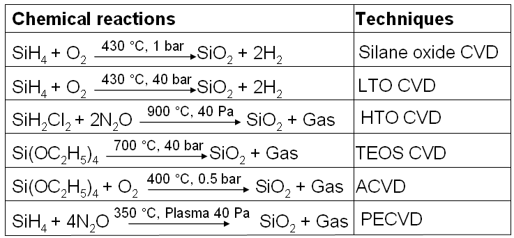
* PECVD: plasma-enhanced CVD; TEOS: tetra-ethyl-ortho-silicate; HTO: high temperature oxide; LTO: low temperature oxide. Table 2075c. Chemical reactions used in CVD for SiO2 film growth.
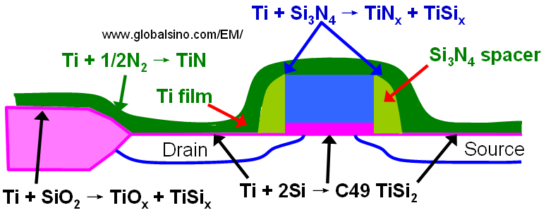
* ACVD: Subatmospheric CVD. Figure 2075a shows several chemical reactions occurring during annealing of a transistor structure coated with Ti to form a low resistive TiSi2 layer at the source, gate, and drain. When silicon and titanium are reacted, Ti and Si can diffuse laterally over the isolation regions and form thin filaments of TiSix that can electronically connect a gate electrode and source/drain regions and can cause failure of the device. This phenomenon is called "bridging". On the other hand, those by-products (TiSix, TiOx, and TiN) form over the isolation regions and cannot easily be etched in conventional salicide etching solutions. The use of a nitrogen atmosphere during thermal annealing is essential in preventing this failure mechanism [1] because nitrogen quickly diffuses into the grain boundaries and significantly suppresses any long-range silicon diffusion in the titanium layer. Furthermore, to avoid the by-product formation, the annealing temperature cannot be too high.
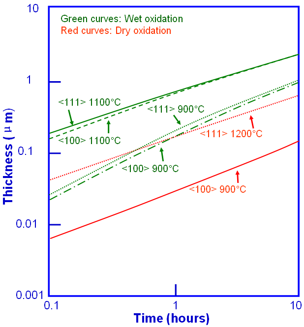
Figure 2075a. Several chemical reactions occurring during annealing of a transistor structure coated with Ti to form a low resistive SiTi2 layer. Figure 2075b shows the dry and wet growth rates on <111> and <100> crystalline silicon (Si) substrates at different elevated temperatures. Two important properties are clearly presented here:
Figure 2075b. Dry and wet growth rates on <111> and <100> crystalline Si substrates. Table 2075d. Etchants used in semiconductor manufacturing.
Table 2075e. Etching selectivity of Si3N4:SiO2:Si in various solutions.
Table 2075f. Etching rate of SiO2 in various solutions.
Si is easily oxidized in air during mechanical polishing for EM analysis. In some critical analyses (e.g. Si surface plasmon analysis) in EELS, Si TEM specimens are normally dipped in HF solution (e.g. 10% HF solution) to remove the surface oxide. However, a thin layer of SiOx may still exist due to exposure to air before loading into the TEM. SiO2 can be in both amorphous and crystalline phases. Table 2075g lists the different forms of SiO2. Table 2075g. Different forms of SiO2.
Table 2075h. Color chart for SiO2 films observed perpendicularly under daylight fluorescent lighting.
Note that substantial local atomic order is still present in fully amorphous silica glass: Each silicon (Si) atom is tetrahedrally surrounded by four oxygen (O) atoms at 1.62 Å, and the oxygen–oxygen separation is typically 2.65 Å. This phenomenon is call short-range ordering.
[1] C. K. Lau, “Method of Forming Titanium Disilicide,” U.S. Patent 4,545,116, 1985.
|
|||||||||||||||||||||||||||||||||||||||||||||||||||||||||||||||||||||||||||||||||||||||||||||||||||||||||||||||||||||||||||||||||||||||||||||||||||||||||||||||||||||||||||||||||||||||||||||||||||||||||||||||||||||||||||||||||||||||||||||||||||||||||||||||||||||||