Chapter/Index: Introduction | A | B | C | D | E | F | G | H | I | J | K | L | M | N | O | P | Q | R | S | T | U | V | W | X | Y | Z | Appendix
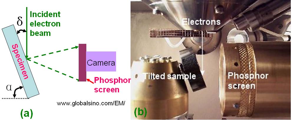
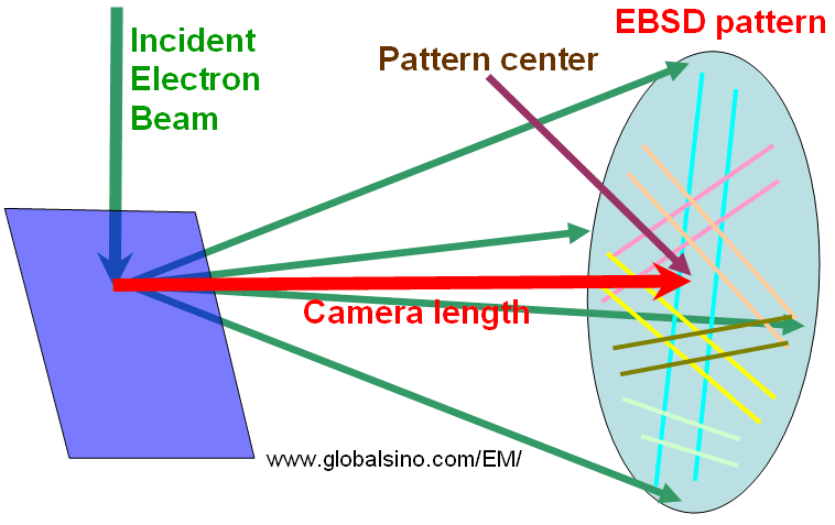
| Electron backscatter diffraction (EBSD) (also known as backscattered Kikuchi diffraction, BKD) is a very powerful method to obtain crystallographic information from samples in the scanning electron microscope (SEM) and provides quantitative microstructural information about most inorganic crystalline materials such as metals, minerals, semiconductors, and ceramics. This technique can be used to analyze grain size, texture, grain boundary misorientations, to map grain orientation in polycrystalline materials, to discriminate between different materials, to provide information about local crystalline perfection, to evaluate the plastic and elastic strain in crystals, and to identify the phase of crystallites by crystallographic point group or space group classification. EBSD had been especially used in metallurgy. In recent years, EBSD has become a well established, routine and easy technique for the SEM. In EBSD measurements, a stationary electron beam with an accelerating voltage of 15 – 25 kV strikes a well-polished crystalline sample tilted at an angle of α (normally 60°-80° with respect to the primary electron beam) and at working distance of 8 – 45 mm. The large sample tilt is to increase the quality of the diffraction patterns. The diffracted electrons form a pattern on a phosphor screen as shown in Figure 2332a. This pattern is characteristic of the crystal structure and orientation of the sample region from which it was generated. Figure 2332a (b) shows an actual EBSD system. Figure 2332b shows EBSD geometry together with camera length (L). The camera is normally placed horizontally so that it is close to the SEM sample for capturing a wide angle of the diffraction patterns.
Figure 2332a. (a) Schematic illustration of EBSD measurement and (b) an actual EBSD system.
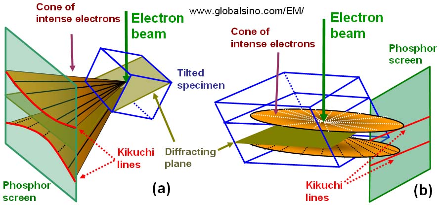
Figure 2332b. EBSD geometry together with camera length (L). An EBSD pattern consists of a number of Kikuchi bands. Each band comprises a pair of parallel Kikuchi lines. The incident electron beam is directed to the point of interest (POI) on the sample surface and thus, the elastic scattering of the electron beam induces the electrons to diverge from a point just below the sample surface and to impinge on crystal planes in all directions. Backscattered electrons that satisfy Bragg's law for a given plane generate two diffraction cones from the front and back surfaces of the plane. These cones are produced for each family of lattice planes. When these cones intersect the phosphor screen or camera thin bands are formed. These bands are called Kikuchi lines. The Kikuchi lines appear as almost straight lines because the cones are very shallow due to the small Bragg angle (order 1°) with a very small electron wavelength. EBSD software can automatically analyze the individual Kikuchi lines by comparing them with the theoretical Kikuchi lines in database. For better understanding, Figure 2332c (a) and (b) shows the formation of Kikuchi lines and electron backscatter diffraction pattern in different ways.
Figure 2332c (a) and (b). The formation of Kikuchi lines and electron backscatter diffraction pattern in different ways.
|