Chapter/Index: Introduction | A | B | C | D | E | F | G | H | I | J | K | L | M | N | O | P | Q | R | S | T | U | V | W | X | Y | Z | Appendix
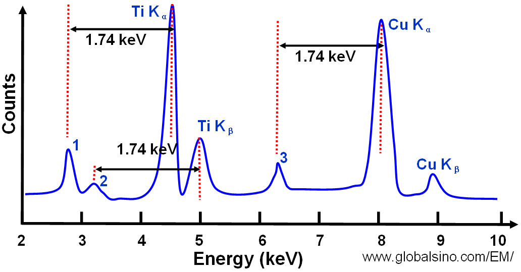
| Crystalline silicon (Si) materials are often used in X-ray detectors (see EDS detectors). Escape peaks occur when a Si X-ray produced by fluorescence escapes the detector, resulting in an artificial peak at an energy equal to the energy of the parent peak minus the energy of the generated Si X-ray (mainly the principal Si-Kα at 1.74 keV). The escape peak is originated from the loss of an Si Kα peak during the photon energy-to-charge conversion process in EDS detector. In practice, there is a statistical probability that some of the x-rays, emitted from the EM sample can interact with Si K-shell electrons in the detector. That is, for a photon of the x-rays with energy higher than the Si K absorption edge, the photon can knock out some Si K-shell electrons in the detector and involves a process of secondary x-ray generation (generating Si K x-ray) in the detector itself. There will not be an impact on the detected signal if this process still contributes to the overall charge collected for the original incident x-ray photon from the EM sample. However, there is a probability that the generated Si Kα x-rays escape from the detector volume and do not contribute to the charge collected for the original photon that is detected. The resulting energy detected for the original photon is reduced by ~1.74 keV (the energy of Si Kα x-ray), showing a new peak. The Si K x-rays can easily escape from the detector crystal if the generation location is close to the front of the detector crystal. The x-rays which generate Si K x-rays far within the volume, will all be absorbed before they can escape from the outer surface of the detector crystal. On the other hand, the probability generating Si Kβ x-rays and of escaping is as low as noise so that we can ignore their escape. The Si Kα escape process results in a peak, in the collected spectrum, with energy of 1.74 keV lower than the parent peaks of the analyzing materials. Figure 3804 shows the schematic illustration of the Si escape peaks 1, 2, and 3 for Ti Kα, Ti Kβ, and Cu Ti Kα, respectively. There is no escape peak corresponding to Cu Kβ peak because the Cu Kβ peak is too weak to finally generate enough Si K signal. Therefore, we should not consider the peaks 1, 2, and 3 as real even though sometime they match the energy positions of some elements, but consider, for instance, the sum of intensities of peak 1 and Ti Kα peak as the real Ti Kα intensity.
The escape peak will usually be a very small proportion of the parent peak and will only be visible for very high-count peaks. Furthermore, multiple escape peaks at different energies 1.74 keV lower than the parent peaks of the analyzing materials can also be generated in x-ray spectrum. The energy of the escape peak Eescape is given by,
where,
For instance, if an element produces a primary characteristic X-ray at Eprimary = keV, the escape peak for a silicon detector would appear at 3.26 keV (=5 keV − 1.74 keV). Therefore, this secondary peak at 3.26 keV would be the escape peak. Some factors can affect the escape peak intensity: i) The geometry of the detector and its ability to retain secondary X-rays. ii) The probability of X-ray escape, which is a function of the detector material and thickness. iii) The energy of the incident X-ray relative to the escape energy; higher energies increase the likelihood of escape peaks. On the other hand, escape peaks are typically more intense in Scanning Electron Microscopy (SEM) than in Transmission Electron Microscopy (TEM) when using EDS. This difference in intensity is due to how the sample interacts with the electron beam in each method, affecting the volume and density of X-ray generation:
|