
Chapter/Index: Introduction | A | B | C | D | E | F | G | H | I | J | K | L | M | N | O | P | Q | R | S | T | U | V | W | X | Y | Z | Appendix
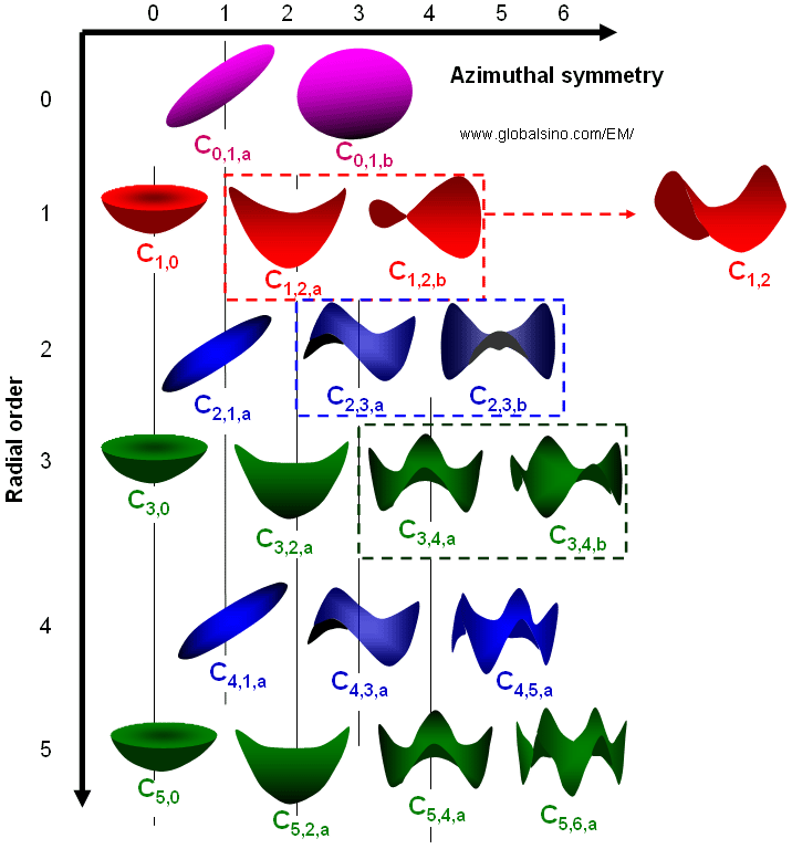
| Optical aberration can be described by the so-called wave aberration functions. There are two types of aberrations: The geometric aberrations are caused by the geometry of the lens electromagnetic field. These aberrations are also called coherent aberrations because they distort the wavefront even though maintain the coherence. For instance, spherical aberration as one type of geometric aberrations was considered by Scherzer. Diffraction is not so much an aberration but the EM resolution still depends on the maximum aperture angle. The geometric aberration G = (Gu, Gv) is given by, [2] The complex expression of the geometric aberration G (= Gu +i Gv) can be given by, The total effect of the coherent aberrations is to extend the distance traveled by the electron wave and thus induce a phase change, χ(k), given by, Figure 4293 shows the aberration coefficients from 0th to 5th order. The vertical lines indicate the groups of different angular symmetries, while the colors of the schematic illustrations in the same rows represent the order of the aberration coefficients. Corresponding to Equation 3740d, in Figure 4293 all the schematic illustrations represent the distortions of the electron wavefronts induced by axial geometric aberrations.
Figure 4293 shows the aberration coefficients from 0th to 5th order. The property of STEM imaging is affected by the geometric aberrations of the probe-forming optics. For instance, for a C5-corrected system where the first-, third- and fifth-order aberrations are set up to optimally oppose uncorrected seventh-order geometric aberrations and the parasitic aberrations up to sixth order are cancelled out, the maximum usable illumination half-angle in STEM can be given by [1],
where,
[1] Krivanek OL, Corbin GJ, Dellby N, Elston BF, Keyse RJ, Murfitt MF, Own CS, Szilagyi ZS, Woodruff JW. An electron microscope for the aberration-corrected era, Ultramicroscopy, 108 (2008) 179–195.
|
 ------------------------- [4293a]
 ------------------------- [4293b]
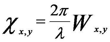
 ------ [4293g]