=================================================================================
In general, a low voltage STEM is a hybrid instrument with the features of SEM and TEM with a convergent probe, while a high voltage TEM is a hybrid instrument with the features of TEM with both a parallel beam (for TEM function) and a convergent probe (for STEM function).
|
SEM |
STEM |
|
=============================== |
=============================== |
Similarity to other techniques |
|
Some are similar to TEM |
|
|
|
Signal |
Secondary electrons (SEs) and backscattered electrons (BSEs) |
Transmitted electrons |
|
|
|
Signal intensity |
Weak intensity from individual atoms due to limited numbers of secondary electrons (or BSEs) from the individual atoms |
Strong intensity from individual atoms due to high transmitted beam intensity |
|
|
|
Source of signal |
The strongest signal is from the top surface: surface-sensitive |
The signal is the integration of the film: probe internal structures directly |
|
|
|
Surface-quality-induced contrast effect |
Allows us to evaluate the atomic arrangement of the few top layers of the sample including the surface quality and condition; a few angstrom-thick amorphous patches greatly reduce the contrast in a SEM image |
Reveals the atomic arrangement of the sample through its entire thickness; a few angstrom-thick amorphous patches do not affect the HAADF image. |
|
|
|
Sensitivity to low-Z elements |
Higher than HAADF STEM imaging (E.g. lattice fringe of carbon nanotubes is visible in Cs-corrected SEM imaging [2]) |
Lower than SEM imaging due to the small scattering cross-section of the light elements (E.g. lattice fringe of carbon nanotubes is invisible in Cs-corrected HAADF imaging [2]) |
|
|
|
Advantages |
Is surface-sensitive and can provide depth (3-D) information |
|
|
|
|
Disadvantages |
|
Gives little 3-D information in the direction of the beam's trajectory |
|
|
|
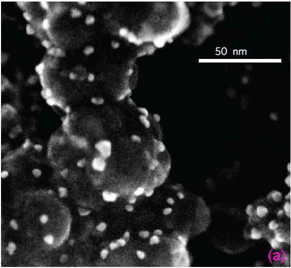
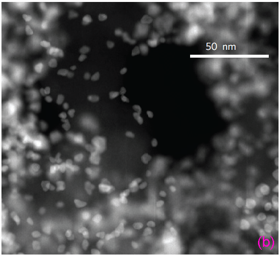
Figure 4447a shows the contrast difference of Pd (Palladium) particles on a thin carbon film. The image (a) using SEs as well as BSEs clearly gives rich depth information, or three-dimensional (3-D) information, about the locations of the particles, while the STEM image cannot give such information.
Figure 4447a. (a) SEM image of Pd nanoparticles on a carbon support obtained using SEs and BSEs; (b) STEM image obained using transmitted electrons (TEs) with an ADF detector.
Adapted from [1].
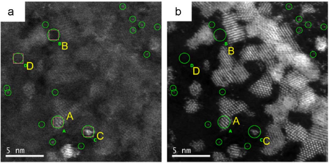
Figure 4447b shows an example of SEM/STEM images taken from uranium oxide particles on carbon film at atomic resolution in both SEM mode and ADF-STEM mode in Cs-corrected Hitachi HD 2700C. It is clear that the contrast of STEM is much better than that of SEM.
Figure 4447b. SEM/STEM images taken from uranium oxide particles on carbon film at atomic resolution in SEM mode (a) and ADF-STEM mode(b).
[2]
Furthermore, the comparison between the EDS measurements in low-energy SEM and high-energy (S)TEM is listed on a table on page4532.
[1] Y. Zhu, H. Inada, K. Nakamura, and J. Wall, Imaging single atoms using secondary electrons with an aberration-corrected electron microscope, Nature Materials, 8 (2009) 808.
[2] H. Inada, D.Su, R. F. Egerton, M.Konno, L.Wu, J.Ciston, J.Wall, Y.Zhu, Atomic imaging using secondary electrons in a scanning transmission electron microscope: Experimental observations and possible mechanisms, Ultramicroscopy 111(2011)865–876.
|