=================================================================================
Charging effect of insulators and some semiconductors in EM (electron microscopy) observations is a well-known phenomenon. Charge-induced SE (secondary electron) contrast is well known in conventional (high vacuum) scanning electron microscopy (SEM) observation of materials, e.g. insulators [1–3], insulator–conductor composites [4], passivated semiconductors [5] and superconductors [6]. This charging phenomenon causes difficulties in the control of charging artifacts, inducing degradations of imaging and spatial resolution [7].
In fact, in a controlled gaseous environment and low vacuum SEM, the effects of inhomogeneous specimen charging on image contrast can be controlled, resulting in stable contrast and utilized for the characterization of a wide range of dielectrics [8].
When the observing structure is electrically isolated, it can be charged during electron irradiation. When the charging process reaches an equilibrium state, the surface potential will maintain constant. In the case of positive charging, the surface potential VS is positive a few volts, retarding the part of the SEs at low-energies and resulting in a lower SE yield. We know that the energy of the SEs is in the range of 0 to 50 eV. Therefore, only the SEs at higher energies can leave from the positive potential surface, leading to a weaker contrast. On the other hand, in the case of negative charging, the negative surface potential slightly retards the incident primary electrons, while it increases the SE yield.
Furthermore, surface charging will, in general, alter the trajectories of all
SEs. This, in turn, will modify the SE
angular-distribution generated from the emitting surface. One example is passive voltage contrast (PVC) in SEM and FIB-secondary electron imaging. The planar area (A) and volume (V) of connected conducting and/or semiconducting materials affect the generation of passive voltage contrast (PVC). For instance, if the connected structure is very large the created charge is not enough to form an electrical potential to significantly affect the trajectory of the generated secondary electrons (SEs). In this case, the contrast of the structure stays bright similar to the structure grounded or stays grey as an electrically leaky contact.
By rough estimation, the radius of the curvature of the SE trajectory is a function of the planar area and volume of the structure (Figure 4568), given by,
r = r (A, V) -------------------------- [4568]
where,
A – The planar area of the connected conducting and/or semiconducting materials
V – The volume of the connected conducting and/or semiconducting materials
Equation 4568 indicates r decreases with A and V. The area A mostly affects the capacitance and electrical leakage of the connected structure, while the volume V mostly affects the charge density in the connected structures. That means, the SE trajectory bends more when A and/or V is smaller. Note that the larger the radius r the more the detected SEs and thus, the brighter the structure.
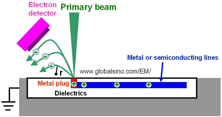
Figure 4568. Schematic illustration of the radius of the curvature of the SE trajectory.
[1] R.D. Van Veld, T.J. Shaffner, in: O.M. Johari (Ed.),
Scanning Electron Microscopy, 1971, p. 17.
[2] J.B. Pawley, in: O.M. Johari (Ed.), Scanning Electron
Microscopy, 1972, p. 153.
[3] T.J. Shaffner, in: O.M. Johari (Ed.), Scanning Electron
Microscopy, 1973, p. 293.
[4] K.T. Chung, J.H. Reisner, E.R. Campbell, J. Appl. Phys.
54 (1983) 6099.
[5] A. Jakubowicz, J. Appl. Phys. 74 (1993) 6488.
[6] K.A. Jenkins, J. Appl. Phys. 70 (1991) 7179.
[7] T.J. Shaffner, in: O.M. Johari (Ed.), Scanning Electron
Microscopy, 1976, p. 61.
[8] T.C. Baroni, B.J. Griffin, J.R. Browne, F.J. Lincoln,
Microsc. Microanal. 6 (2000) 49. |