Chapter/Index: Introduction | A | B | C | D | E | F | G | H | I | J | K | L | M | N | O | P | Q | R | S | T | U | V | W | X | Y | Z | Appendix
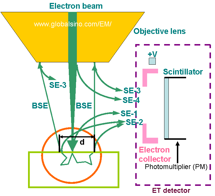
| There are many factors limiting the spatial resolution in electron microscope as discussed on the page of Spatial Resolution in Electron Microscopes. For secondary electron microscopes (SEMs), one of the factors is the source of secondary electrons (SEs) in SEMs. As shown in Figure 4581a, there are four types of SEs collected by one kind of SE detectors, namely Everhart-Thornley (ET) detector. SE1s are generated by direct interaction with the incident (primary) electron beam and therefore carry the highest spatial resolution information because the spatial resolution is mainly determined by the size of the primary electron beam. The spatial resolution of detection of SE2s is poorer because SE2s are induced by multiple scattering of electrons in materials and thus, the spatial resolution is mainly determined by d as shown in Figure 4581a. In 1940, before the first SEM images were collected, yon Ardenne predicted that SE2 would limit resolution, saying because SE2 cannot be detected separately from SE1 [2].
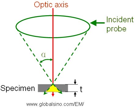
Figure 4581a. Four types of secondary electrons collected by the Everhart-Thornley (ET) detector. Adapted from Reimer [1]. In scanning electron microscope (SEM), spherical aberration of the probe-forming lens is increased with the increase of working distance, resulting in a larger electron-probe size. Therefore, the need to have better spatial resolution of SEM leads to shorten the working distance and consequently to change the SEM detector position. Furthermore, as shown on the page of Electron Beam Diameter, any change in the working distance or diameter of the aperture defining α or in the beam intensity, i, dramatically deteriorates the optimum value of the lateral resolution. Furthermore, Figure 4581b shows the schematic illustration of interaction volume with a thin film as the SEM specimen. It is clear that the interaction volume is larger when the semi-convergence angle of the SEM probe is larger, and thus the SEM spatial resolution will be affected. Therefore, in order to optimize the spatial resolution, it is important to balance the following factors:
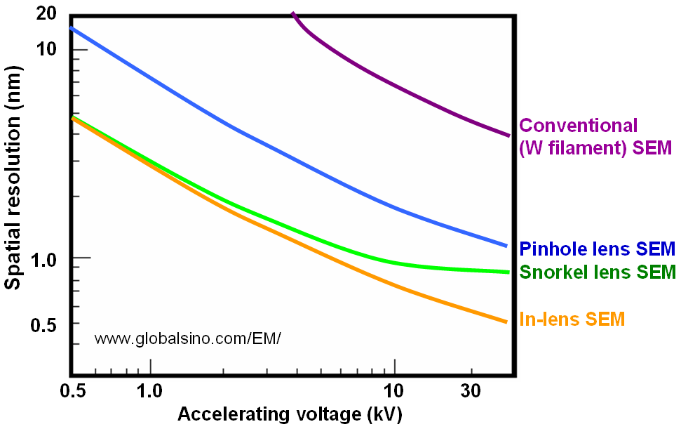
Even for primary electrons of zero diameter, the profile of secondary electrons normally has a range of more than 15 nm [5]. This profile affects the spatial resolution of SEM. In SEM observations, the best spatial resolution is 0.4 nm obtained at 30 kV in Hitachi S-5500 without aberration correction [3] and is 0.6 nm at 5 kV in JEOL JSM-7700F with aberration correction [4]. Figure 4581c shows the schematic illustration of spatial resolutions of SEMs with various lenses, including conventional W (tungsten) filament SEMs, pinhole lens, snorkel lens, and in-lens. The best resolution can be obtained by in-lens SEMs.
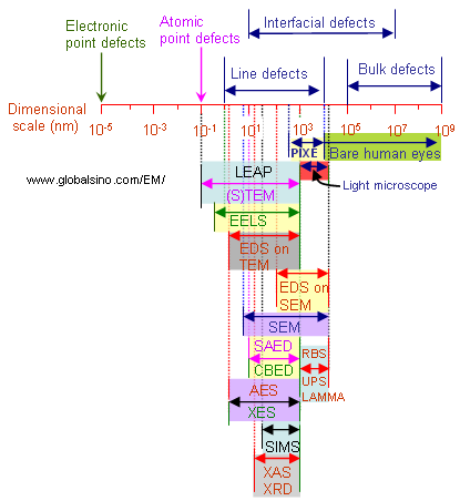
Figure 4581d shows the typical sizes of various material defects and the capability of analytical techniques (See the full names of the techniques at page3928). The lowest levels of the techniques represent their spatial resolutions.
Figure 4581d. Typical sizes of various material defects and capability of analytical techniques.
[1] Reimer, L., Scanning Electron Microscopy, Springer Verlag, New York, 1985.
|
|||||