Sample Thickness Determination using EELS
- Practical Electron Microscopy and Database -
- An Online Book -
Electron microscopy
  Microanalysis | EM Book                                                                   http://www.globalsino.com/EM/  


As we know that in TEM observation, the transmission of unscattered incident electrons is inversely proportional to the TEM specimen thickness. On the other hand, the increase of the specimen thickness enhances the energy loss of the transmitted electrons. Therefore, the spatial resolution degrades with the increase of specimen thickness because of the chromatic aberration effects. Table 4621a lists examples of the energy loss of incident electrons passing through the specimen. The use of thinner specimen can generally improve spatial resolution because it minimizes the energy loss.

Table 4621a. Examples of the energy loss of electrons passing through the TEM specimen.

  Accelerating voltage of incident electrons Penetrated electrons (%) Penetrated electron with energy loss higher than 50 eV (%) Unscattered electrons (%) Elastically scattered electrons (%)
Thin metal foil
50
40
50 nm thick carbon film
50 kV
55
33
10

For many solids, especially metals, the bonding electrons can be considered as a free electron gas. Plasmons that are oscillations of the free electrons are generated when an incident electron travels through the gas. Plasmon spectra are routinely used to measure the thickness of a TEM specimen because more plasmons are excited as the electron goes through a thicker specimen. If diffraction effects are negligible, thickness t of TEM samples can be evaluated as a multiple of the inelastic mean free path using log-ratio
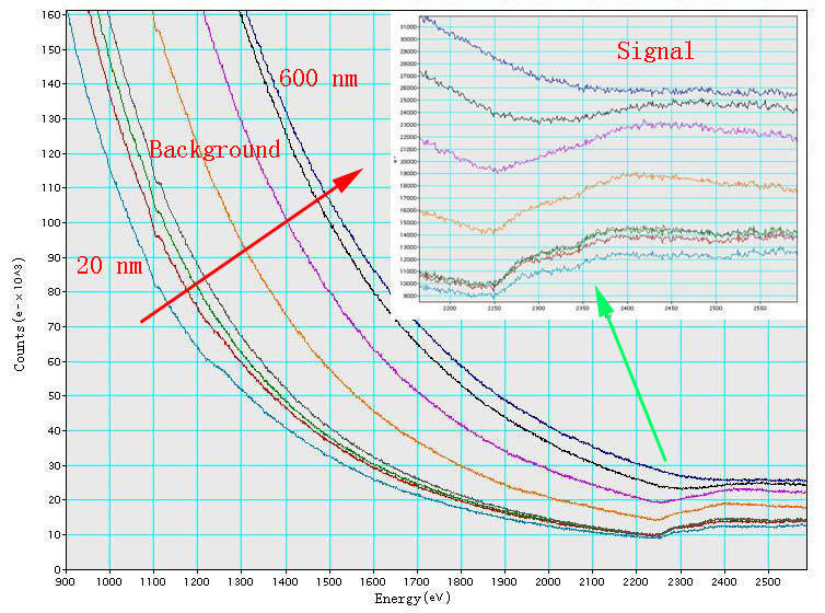
 method [1, 10-11]:
         measure the TEM sample thickness using EELS ------------------- [4621a]
where,
         λ -- The mean free path of the inelastic scattering (due mainly to valence electrons).
         It -- The integral of total spectrum counts (zero-loss peak plus extrapolated loss part), the total number of electrons in the EEL spectrum, or called the total unfiltered image intensity. To capture most of the intensity, It need only be integrated up ~200 eV for TEM specimens of t < 200 nm. For thicker TEM specimens, the spectrum can be extrapolated until the spectral intensity becomes negligible. [12]
         I0, -- The integral of zero-loss peak counts (e.g. between -3 and 3 eV), or called the number of electrons having lost no energy.

The cross-section of the scattering can be extracted by the relation,
         1/λ = Nσ -------------------------- [4621b]
where,
         N = ρ/(Am)
         N -- The atomic density,
         ρ -- The mass density,
         A -- The dimensionless atomic mass,
         m -- The proton mass.

The mean free inelastic path of electrons ( λ) has to be measured or calculated by an independent method. In practice, It can be replaced by Ip, which is the integral of the low-loss spectrum (e.g. between −3 and 97 eV). This calculation process can be performed with some software, for instance, Gatan digital micrograph (DM). Note that an appropriately modified form of the relationship in Equation 4621a should be applied if the plural scattering has been removed from the spectrum.

For the case of EFTEM, similar to Equation 4621a, two intensity maps are acquired: one is formed by all transmitted electrons (intensity It , unfiltered image), the other one by selecting only those electrons that did not lose any energy (intensity I0, filtered image). The relative drift between the unfiltered and filtered images was corrected by a standard cross-correlation technique when computing the ratio map It /I0.

Furthermore, to accurately evaluate TEM specimen thicknesses, both surface and bulk plasmons need to be considered. However, in calculations, we normally consider that only the bulk effect contributes to the plasmon-loss in specimens thicker than 150 nm. The surface plasmon-loss (Is) has dependence on TEM-specimen thickness only when the specimen is extremely thin (e.g. <10 nm in general). On the other hand, for very thin TEM specimens, e.g. ≤30 nm for Si (or ≤0.25 λP), several surface-induced effects contribute to plasmon signal:
         i) Radiative surface plasmons [2] locate just above bulk plasmon energies (EP).
         ii) Coupling of surface plasmons [3] excited at the two surfaces.
         iii) Coupling of surface and bulk plasmon excitation [4].
         iv) Errors in calculations in the energy region of EP to 2EP due to angular effects. These errors are not considered in the Fourier-log deconvolution process that is the method normally used in the calculations.

The peak-to-background ratio in EELS varies with specimen thickness so that it also can be used to determine the specimen thickness. For instance, Figure 4621a shows that the background increases dramatically with increase of the thickness of TEM specimen, while the signal of Pt M4,5 edge decreases significantly. In this case, the highest signal in the range of these TEM specimen thicknesses for Pt occurs at 20 nm. However, in the method with peak-to-background ratio, a correlation curve between the ratio and thickness should be plotted and used to calibrate the interesting thickness.

EELS of Pt M4,5 edg

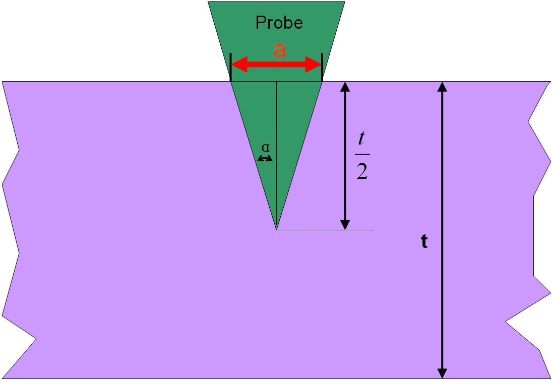
Figure 4621a. EELS of Pt M4,5 edge.

Furthermore, the "local" EELS intensity also depends on the spatial resolution of STEM, which is especially important for measurements of multi-layers. It is necessary to mention that the spatial resolution of the measurements in STEM mode can be estimated by the diameter of the probe irradiation on the specimen, given by (see Figure 4621b):
          Spatial Resolution due to Specimen Drift -------------------------------- [4621d]
where,
          α -- The convergence semiangle,
          t -- The thickness of the specimen.

Diameter of the probe irradiation with specimen thickness t

Figure 4621b. Diameter of the probe irradiation with specimen thickness t.

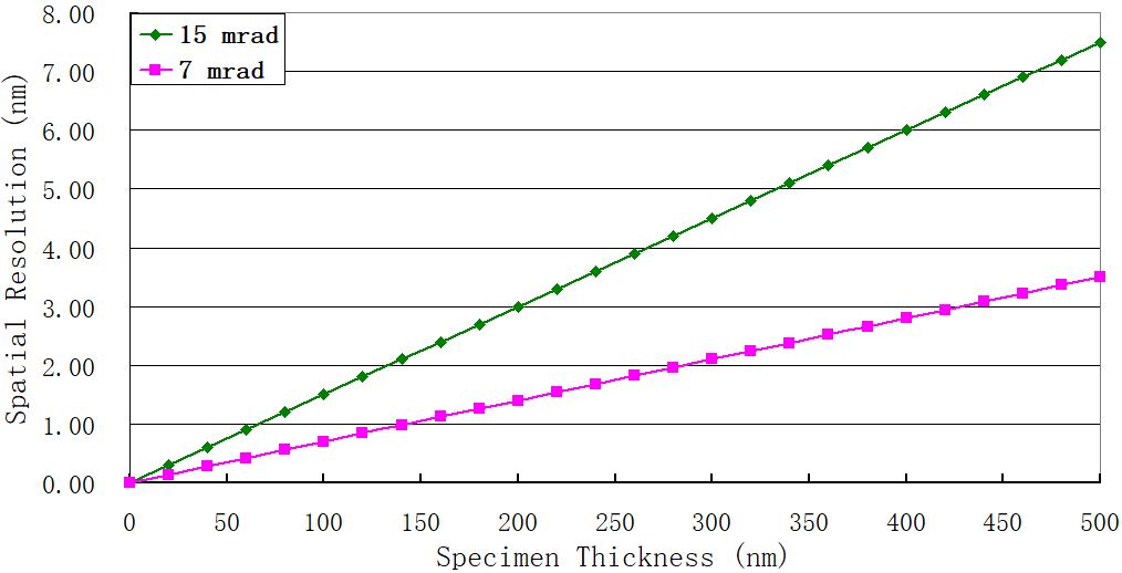
For instance, Figure 4621c shows the spatial resolutions at convergence semiangles 7 and 15 mrad, respectively, based on Equation 4621d. Note that such convergence semiangles are used in many TEM systems.

Examples of drift effect on spatial resolution
Figure 4621c. Spatial resolutions at convergence semiangles 7 and 15 mrad, respectively, based on Equation 4621d.


Table 4621b. Comparison between various thickness measurement methods based on EELS proposed by different researchers. [5]
Methods Small collection semiangles Medium collection semiangles Large collection semiangles
Kramers–Kronig sum-rule method (with correction for plural and surface scattering) Overestimates the thickness due to underestimation of the surface-mode scattering 10 % accuracy  
Log-ratio method (with Equation [4621a]) Within 10% for t/λi < 5 in amorphous, polycrystalline, and single-crystal specimens [8-9]
10 % accuracy with a formula for inelastic mean free path proposed by Malis et al. [6] Preferable with a formula for inelastic mean free path proposed by Iakoubovskii et al. [7]


[1] Egerton, R.F. (1996). Electron Energy Loss Spectroscopy in the Electron Microscope. New York: Plenum Press.
[2] R. Vincent, J. Silcox, Phys. Rev. Lett. 31 (1973) 1487.
[3] R.B. Pettit, J. Silcox, R. Vincent, Phys. Rev. B 11 (1975) 3116.
[4] C.H. Chen, J. Silcox, R. Vincent, Phys. Rev. B 12 (1975) 64.
[5] Huai-Ruo Zhang, Ray F. Egerton and Marek Malac, Local thickness measurement through scattering contrast and electron energy-loss spectroscopy, Micron 43 (2012) 8–15.
[6] Malis, T., Cheng, S.C., Egerton, R.F., 1988. EELS log-ratio technique for specimenthickness measurement in the TEM. J. Electron Microsc. Technol. 8, 193–200.
[7] Iakoubovskii, K., Mitsuishi, K., Nakayama, Y., Furuya, K., 2008. Thickness measurements with electron energy loss spectroscopy. Microsc. Res. Technol. 71, 626–631.
[8] Hosoi, J., Oikawa, T., Inoue, M., Kokubo, Y., and Hama, K. (1981) Measurement of partial specific thickness (net thickness) of critical-point-dried cultured fibroblast by energy analysis. Ultramicroscopy 7, 147–154.
[9] Leapman, R. D., Fiori, C. E., and Swyt, C. R. (1984a) Mass thickness determination by electron energy-loss for quantitative x-ray microanalysis in biology. J. Microsc. 133, 239–253.
[10] Joy, D.C., Egerton, R.F., and Maher, D.M., Progtra. In: Scanning Electron Microscopy. SEM Inc., AMF O’Hare, Illinois, part 2, pp. 817-826 (1979).
[11] Leapman, R.D., Fiori, C.E., and Swyt, C.R., Mass thickness determination by electron energy-loss for quantitative x-ray microanalysis in biology. J. Microsc., 133:239-253 (1984).
[12] R.F. Egerton, Electron Energy-Loss Spectroscopy and Nanoanalysis (TEM-EELS).


;