Chapter/Index: Introduction | A | B | C | D | E | F | G | H | I | J | K | L | M | N | O | P | Q | R | S | T | U | V | W | X | Y | Z | Appendix
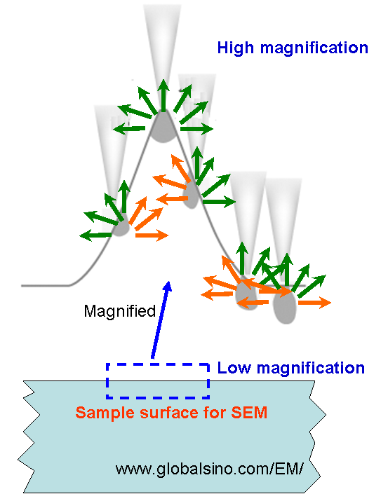
| The contrasts of SEM images can be basically categorized by topographic, material, and voltage contrast. The surface topographic contrast is utilized most frequently in SEM observations comparing with other SEM contrasts. This contrast originates from the difference of the SE yield for different incident angles of primary electrons irradiating a specimen surface. The surface topography of a specimen dictates the SEM contrast changes that portray the specimen image. As shown in Figure 4860, the sample surface probably is not flat (top image) at a high magnification even though it seems flat at a low magnification (bottom image). The contrast at peaks of the topography is enhanced by the efficient electron emission from the peaks as indicated by the green arrows. However, the some SEs cannot come out from the sample due to bulk effect of the materials in flat or slope regions as indicated by the orange arrows. In this case, the measured SEs are highly sensitive to surface topography so that they are more likely collected from the peaks than the valleys of the surface. The difference of emission volume (roughly equals to interaction volume) of SEs (secondary electrons) can be very small from location to location; however, the contrast can be very different due to topography.
Figure 4860. topographic effect on SEM contrast This phenomenon can be especially true for nanoparticles sitting at a flat surface when you are observing nanoparticles in SEM. This artifact actually can also be an advantage of SEM method when you want to observe nanoparticles which have very low nature SEM contrast from bulk materials. That is, you would like to intentionally disperse the nanoparticles on a flat substrate surface instead of burying in bulk materials. The convex and trench structures and groove edges generate brighter signals in the topographic contrasts. For instance, microelectronics industry uses the topographic contrast to perform the detection of the strip width, side wall, profile analysis, critical-dimension (CD), overlay measurement, etc. Furthermore, a low take-off angle (α) is more sensitive to topographic effects. For this reason, secondary electron detectors are located at low angles to enhance the topographic resolution of secondary electron images.
|