Spherical Aberration Correctors
- Practical Electron Microscopy and Database -
- An Online Book -

https://www.globalsino.com/EM/  


This book (Practical Electron Microscopy and Database) is a reference for TEM and SEM students, operators, engineers, technicians, managers, and researchers.


=================================================================================

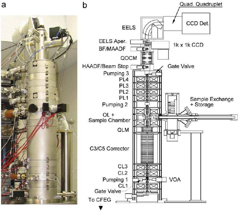
Spherical Aberration (Cs) correction was first introduced by Rose [1,2] However, due to the need for high mechanical precision and lens current stability, as well as for computer control, Cs correctors had not been achieved until the end of the 20th century [3, 4]. The first practical aberration corrector was installed on a test bench to verify the applicability of Cs correction [12]. The demonstration setup on a modified SEM included a Cs corrector entirely incorporated into a specimen chamber and a CCD camera coupled with a scintillator underneath the specimen chamber. The electron probe was focused on the scintillator, and scanned circularly with a series of diameters so that the ray displacements induced by the aberration corrector could be observed.

In scanning TEM, the resolution-limiting factor is the size of the focused electron probe. As shown in Equation [4954d], the beam size can be reduced by minimizing Cs. With use of Cs correctors, it was demonstrated that probe size below 0.1 nm can be achieved [5 - 8]. An important advantage of Cs correctors is that larger acceptance angles can be used that increase the probe current considerably. In the TEM, Cs correctors allow for a much more straightforward interpretation of high-resolution images. Furthermore, a negative Cs value of objective lens has been applied in materials studies. For instance, this technique simplified the detection of light atoms [9] and enabled to image all types of atomic columns in the dielectric SrTiO3 and the superconductor YBa2Cu3O7 [10].

Spherical aberration correctors combine multipoles and rotational symmetry lenses. The example in Figure 4945 shows a TEM system facilitated with a C3/C5 corrector for spherical aberration corrections. Note that different from most commercial TEM systems (see schematic diagram of TEM systems), this TEM system without phosphor screen has the incident electrons emitted from the bottom of the systems and the detectors on the top.

schematic cross-section of the column.


【*】 Detectors: HAADF, BF, EELS

【*】 QOCM: Quadrupole/octupole module called quadrupole–
octupole
coupling module

【*】 Four round projector lenses: PL1, PL2, PL3, and PL4.

【*】 OL: Objective lens

【*】 QLM: Quadrupole lens module

【*】 C3/C5 corrector: quadrupole–octupole C3/C5 corrector

【*】 Three round condenser lenses: CL1, CL2, and CL3

【*】 CFEG: Cold field emission gun

Figure 4945. (a) The TEM column and (b) Schematic cross-section of the column. [11]


[1] Rose H. 1990. Outline of a spherically corrected semiaplanatic medium-voltage transmission electron-microscope. Optik 85:19–24
[2] Rose H. 1999. Prospects for realizing a sub-Å sub-eV resolution EFTEM. Ultramicroscopy 78:13–25
[3] Haider M, Rose H, Uhlemann S, Schwan E, Kabius B, Urban K. 1998. A spherical-aberration-corrected 200 kV transmission electron microscope. Ultramicroscopy 75:53–60
[4] Krivanek OL, Dellby N, Lupini AR. 1999. Towards sub-Å electron beams. Ultramicroscopy 78:1–11
[5] Haider M, Uhlemann S, Zach J. 2000. Upper limits for the residual aberrations of a high-resolution aberration-corrected STEM. Ultramicroscopy 81:163–75
[6] Krivanek O, Nellist P, Dellby N, Murfitt M, Szilagyi Z. 2003. Towards sub-0.5 Å electron beams. Ultramicroscopy 96:229–37
[7] Batson P. 2003. Aberration correction results in theIBMSTEMinstrument. Ultramicroscopy 96:239–49
[8] Nellist P, Chisholm M, Dellby N, Krivanek O, Murfitt M, et al. 2004. Direct sub-Angstrom imaging of a crystal lattice. Science 305:1741
[9] Urban K, Kabius B, Haider N, Rose H. 1999. A way to higher resolution: spherical-aberration correction in a 200 kV transmission electron microscope. J. Electron Microsc. 48:821–26
[10] Jia C. L., Lentzen M., Urban K., 2003. Atomic-Resolution Imaging of Oxygen in Perovskite Ceramics, Science 299:870-873
[11] Krivanek OL, Corbin GJ, Dellby N, Elston BF, Keyse RJ, Murfitt MF, Own CS, Szilagyi ZS, Woodruff JW. An electron microscope for the aberration-corrected era, Ultramicroscopy, 108 (2008) 179–195.
[12] Haider, M., Braunshausen, G. & Schwan E. (1995). Correction of the spherical aberration of a 200 kV TEM by means of a Hexapole-corrector. Optik 99, 167–179.


=================================================================================

The book author (Yougui Liao) welcomes your comments, suggestions, and corrections, please click here for submission. If you let book author know once you have cited this book, the brief information of your publication will appear on the “Times Cited” page.