Chapter/Index: Introduction | A | B | C | D | E | F | G | H | I | J | K | L | M | N | O | P | Q | R | S | T | U | V | W | X | Y | Z | Appendix
| Titanium disilicide (TiSi2) is a form of TiSix materials. TiSi2 is a refractory metal silicide commonly applied as interconnects in ultra-large-scale integrated (ULSI) circuits and as gate electrodes in metal–oxide–semiconductor (MOS) transistors [1 - 2] because of its low resistivity, thermal stability and excellent electrical contact properties with silicon [3 - 5]. TiSi2 among the refractory metal silicides shows the lowest resistivity (~12.4 µΩ cm). Table 150a. Properties of TiSi2 materials.
Table 150b. Comparison of the properties of CoSi2 and TiSi2.
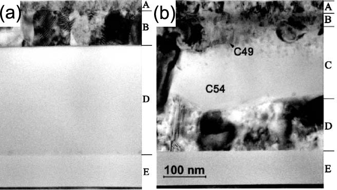
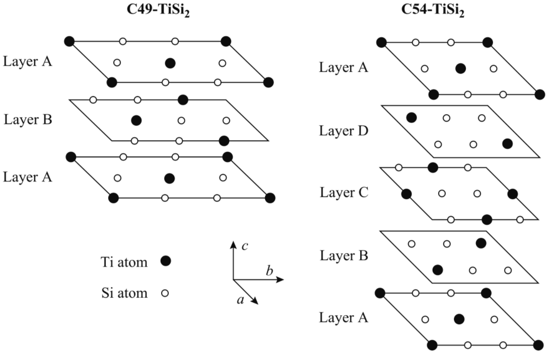
The TiSi2 formed by solid state reaction of between Ti and Si films has two different structures: the C49 (base-centered orthorhombic) structure formed between 450 °C and 650 °C, and the C54 (face-centered orthorhombic) structure formed above 650 °C. The C49 TiSi2 is a metastable phase and is usually the first crystalline phase to form in the reaction between Ti and Si, while the C54 TiSi2 phase is a stable phase, having a lower electrical resistivity than the C49 phase. Both crystal structures have similar atomic arrangements with a hexagonal array of Si atoms around Ti atoms at the center, but the staking arrangement of the unit cells are different: the C49 phase has a two-layer repeat while the C54 phase has a four-layer repeat. C54 TiSi2 has orthorhombic structure and has 24 atoms per unit cell. The C49–C54 transition temperature increases as the Ti film thickness decreases and varies as a function of substrate orientation [6] and stress The C49 TiSi2 present an anisotropic thermal expansion coefficients: the αb is considerably smaller than αa and αc because of the presence of Assuming Ti (titanium) film is first deposited on a Si substrate, the free energy of the system will change if the Ti atoms react with the Si atoms to form titanium silicide (TiSi2) film. To form a TiSi2 layer in thickness t, 0.4t of the Ti film and 0.9t of the Si substrate need to be consumed. Therefore the free energy change ΔG to form the TiSi2 layer is, Note that the driving force for the C49 to C54 transition is the energy differences of G0TiSi2, γTiSi2/Si, and γTiSi2. for the two phases. Under some conditions, prior to the disilicide formation [8-10], the initial crystalline phase formed during the Ti–Si interaction is a metal-rich silicide (either Ti5Si3 or Ti5Si4). Then, the disilicides form at the expense of the metal-rich silicide at higher annealing temperature. The TEM images in Figure 150a shows the stacking structures before and after annealing at 900 K. The layers A, B, C, D, and E are capped TiN, deposited Ti, TiSi2, amorphous Si (for (a)) or polycrystalline Si (for (b)), and SiO2, respectively. The as-deposited TiN film has a columnar texture and is preferentially oriented with (111) planes parallel to the surface. After annealing, a TiSi2 layer with mixed C49 (close to the TiN layer) and C54 (close to the polycrystalline Si layer) phases is formed.
Figure 150a. TEM images of the stacking structures before (a) and after (b) annealing at 900 K.
Adapted from [16]
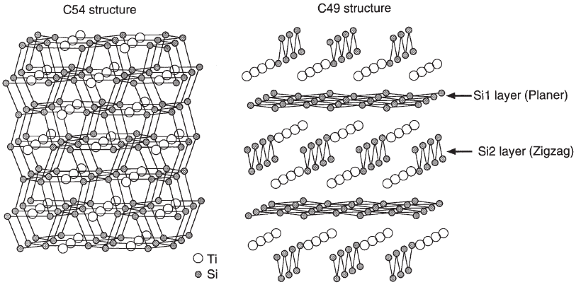
Figure 150b shows the atomic arrangement of the two TiSi2 crystals C49 and C54. TiSi2 C49 has two Si sites: Si1 and Si2. Si1 is in the form of a two-dimensional hexagonal sheet, while Si2 forms a zigzag chain. In both C49 and C54, only the nearest-neighbor Si–Si bonds are connected.
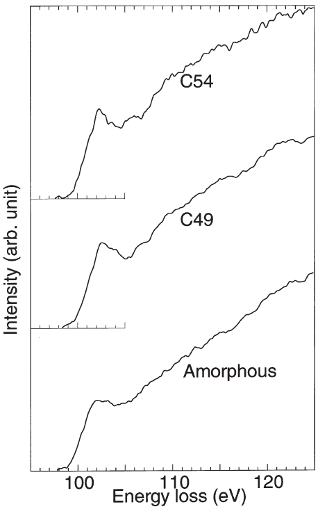
Figure 150d shows experimental ELNES spectra at the Si-L2,3 edge taken from amorphous, C49, and C54 TiSi2. All the three spectra consist of a small peak located at around 102 eV superposed on a very broad peak. The clear difference between three spectra is the width of the first peak. This peak is sharper in the C54 sample than in the C49 sample, while the amorphous sample is similar to the C49 sample.
Figure 150d. Experimental Si-L2,3 edge ELNES spectra taken from amorphous, C49, and C54 TiSi2.
[17]
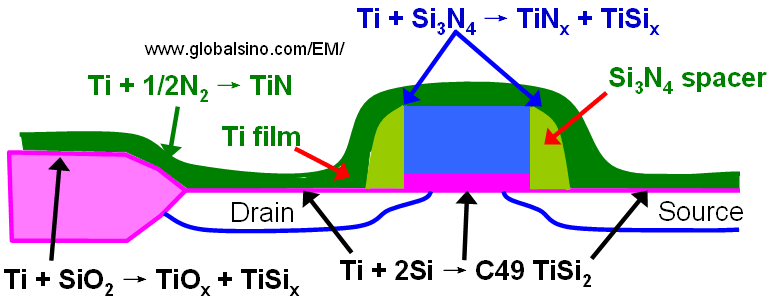
Note the experimental ELNES spectra at the Ti-L2,3 edge taken from amorphous, C49, and C54 TiSi2 are very similar. Figure 150e shows several chemical reactions occurring during annealing of a transistor structure coated with Ti to form a low resistive TiSi2 layer at the source, gate, and drain. When silicon and titanium are reacted, Ti and Si can diffuse laterally over the isolation regions and form thin filaments of TiSix that can electronically connect a gate electrode and source/drain regions and can cause failure of the device. This phenomenon is called "bridging". On the other hand, those by-products (TiSix, TiOx, and TiN) form over the isolation regions and cannot easily be etched in conventional salicide etching solutions. The use of a nitrogen atmosphere during thermal annealing is essential in preventing this failure mechanism [18] because nitrogen quickly diffuses into the grain boundaries and significantly suppresses any long-range silicon diffusion in the titanium layer. Furthermore, to avoid the by-product formation, the annealing temperature cannot be too high.
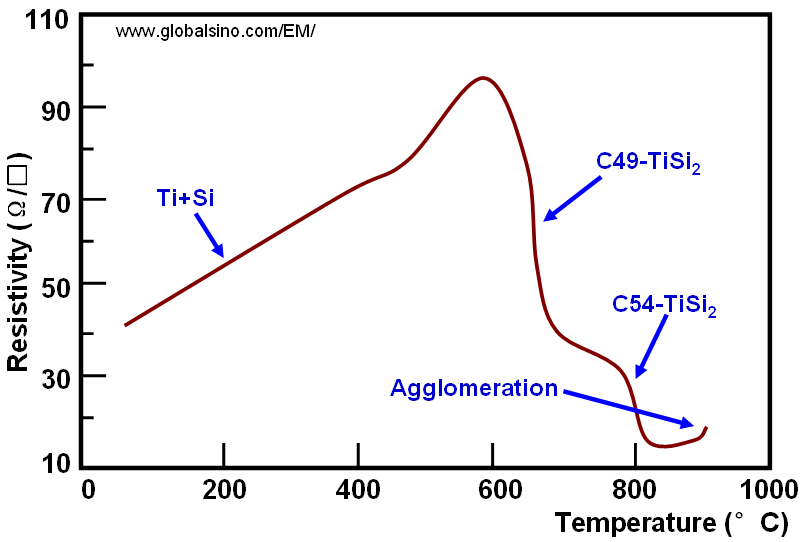
The resistivities of the C49 phase and the C54 phase are very different as shown in Figure 150f so that to form low resistive contacts the phase transformation from C49 to C54 is very important. Figure 150f shows that the resistivity increases because of silicon diffusion into the metal as the temperature is increased from room temperature, while the resistivity reduces abruptly as C49 is formed, followed by further reduction to C54 phase. At temperatures above 900 °C the TiSi2 becomes discontinuous and the resistivity increases due to agglomeration. Therefore, the C54 process window is about 100 °C. On the other hand, the doping, reduced linewidth, and film thicknesses narrows the process window down significantly. Since the transformation is nucleation-limited, the transformation on narrow lines is more difficult. Note that the C54 nucleation density is increased by higher temperature annealing.
Figure 150f. Dependence of phase and resistivity on annealing temperature.
[1] A.A. Bos, N.S. Parekh, A.G.M. Jonkers, Thin Solid Films 197 (1991) 169.
|
||||||||||||||||||||||||||||||||||||||||||||||||||||||||||||||||||||||||||||||||||||||||||||||