Chapter/Index: Introduction | A | B | C | D | E | F | G | H | I | J | K | L | M | N | O | P | Q | R | S | T | U | V | W | X | Y | Z | Appendix
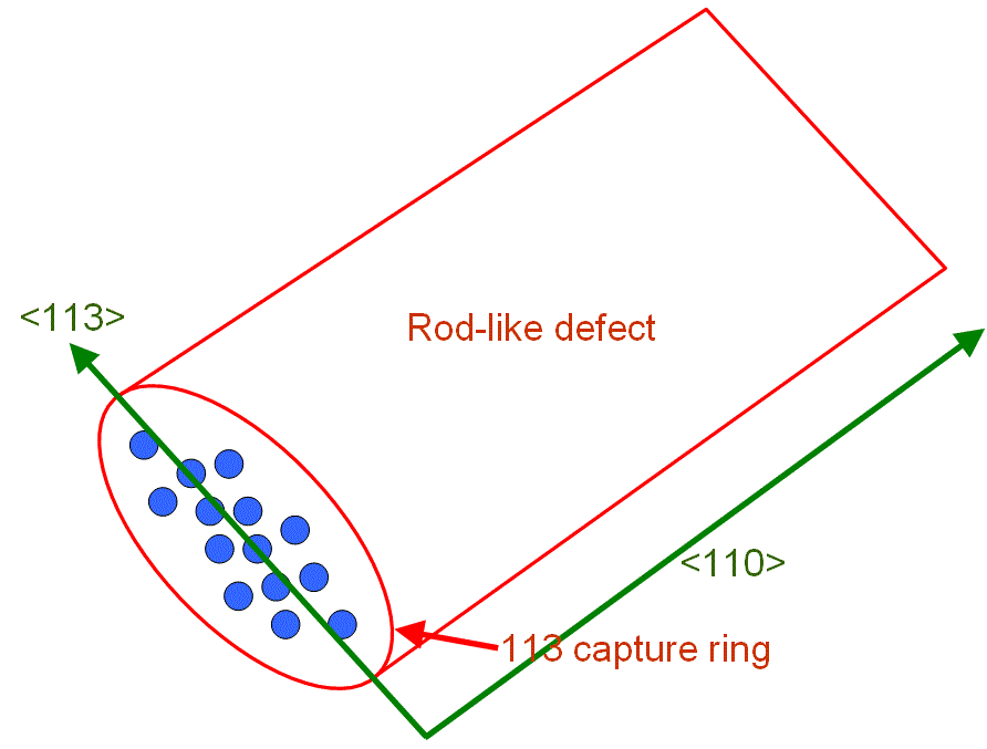
| {113} or {311} defects are extended, rod-like defects. Those defects especially play a central role in the processing of Si (silicon) during integrated circuit (IC) fabrication. Because of the cubic (3 mm) symmetry of fcc, there are 6 possible <110> directions for the defect elongation and 12 possible {113} or {311} habit planes. Figure 1820a shows a formed long interstitial chain on a <113> plane in a <110> direction. It is believed that the {113} plane in the defects is composed of interstitial chains and the interstitials in the {113} rod-like defects form extra "virtual" planes even though the density of the interstitials is not enough to create a full extra plane. The virtual extra {113} plane lies between two {113} lattice planes. The distance between the virtual plane and the two {113} lattice planes, where the virtual plane lies between, equals the Burgers vector.
Figure 1820a. Formed long interstitial chain on a <113> plane in a <110> direction. The blue dots represent the interstitials in the defects. As discussed in the examples in page1819, during higher temperature annealing, the defects in crystals undergo a series of transitions from self-interstitial clusters to {113} defects to dislocation loops. Table 1820. Examples of {113} or {311} defects.
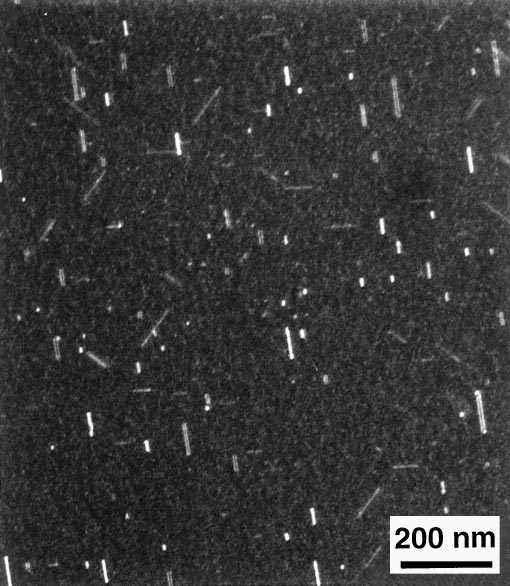
Figure 1820b shows a 040 weak-beam dark-field TEM image of B-implanted Si, presenting rod-like {113} defects. These defects lie on {1 1 3} planes and are elongated along the <1 1 0> directions with a Burgers vector of a/25<1 1 6>. [3]
Figure 1820b. 040 weak-beam dark-field TEM image of B-implanted Si (at a dose of 5 x 1013 cm-2 at 40 keV and annealed at 800 °C. [2]
[1] K. S. Jones, J. Liu, L. Zhang, V. Krishnamoorthy, R. T. DeHoff, Studies of the interactions between (311) defects and type I and II dislocation loops in Si+ implanted silicon, Nuclear Instruments and Methods in Physics Research B, 106 (1995) 227-232.
|