Chapter/Index: Introduction | A | B | C | D | E | F | G | H | I | J | K | L | M | N | O | P | Q | R | S | T | U | V | W | X | Y | Z | Appendix
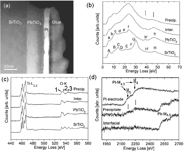
The sandwich structure shown in Figure 2320a (a) is composed of three layers: SrTiO3, PbTiO3, and Pt. An amorphous Ti-rich interfacial layer as well as nanometer size precipitates was formed at PbTiO3/Pt interfaces. In the low-loss region in EELS from the different layers shown in Figure 2320a (b), the energy peaks labeled A–H for SrTiO3 and a–h for PbTiO3 are formed by interband transitions which are typical in bulk SrTiO3 and PbTiO3 [1]. The strong peaks H/h and H’/h’ arise from transitions of Ti 3p to higher energy levels such as Ti 3d, Ti 4s, forming Ti M2,3 edge. In the precipitates, the transitions h and h are reduced in intensity because these precipitates might be Ti-deficient. In Figure 2320a (c), the two core loss EELS profiles from SrTiO3 and PbTiO3 layers show clear splitting of the Ti-L2,3 edges, while for the interfacial layer the splitting at the Ti-L3 edge is much less and the splitting at the Ti-L2 edge disappears. The splitting of Ti-L2,3 edges reflects the hybridization and ligand field strength of Ti–O atomic interaction so that the reduction of splitting in the interfacial layer reflects the weaker Ti–O bonding force. Due to the similar hybridization of O 2p states with Ti 3d in the conduction band, the energy region from 530 eV to 536 eV is split into two subbands t2g (marked peak 1) and eg (marked peak 2). Figure 2320a (d) shows the EEL spectra of Pb- and Pt-M4,5 edges.
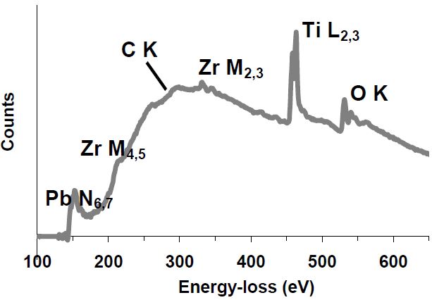
Figure 2320b shows an EEL spectrum taken from a lead zirconate titanate (Pb(Zr0.3Ti0.7)O3, PZT) thin film.
[1] K. V. Benthem, C. Elsasser, and R. H. French, J. Appl. Phys. 90, 6156 (2001).
|