Chapter/Index: Introduction | A | B | C | D | E | F | G | H | I | J | K | L | M | N | O | P | Q | R | S | T | U | V | W | X | Y | Z | Appendix
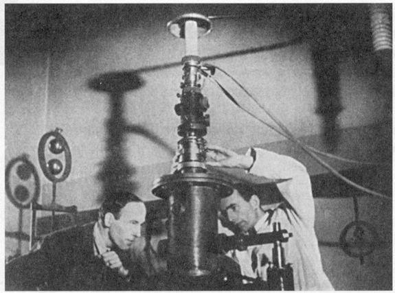
| Knoll and Ruska had built the first TEM system in 1932 (see Figure 4539). Ruska received the Nobel Prize in 1986 for this invention. The first commercial TEMs were developed by UK companies in 1936 and several major companies such as Hitachi, JEOL, FEI/Philips and RCA, inter alia have been producing TEM systems after the end of World War II. In 1949, Heidenreich first thinned metal foils to electron transparency, resulting in the most important development of TEM applications in the field of materials science. This work was followed up by Bollman in Switzerland, and Hirsch and co-workers in Cambridge. Furthermore, the Cambridge group also developed the theory of electron diffraction contrast. Practical applications of TEM for the solution of materials problems were pioneered in the U.S. by Thomas. Other materials-oriented texts followed, e.g., Edington (1976) and Thomas and Goringe (1979).
Figure 4539. The electron microscope built by Ruska and Knoll in Berlin in the early 1930s. For more than 40 years after 1931 all TEMs had been based on Ruska’s design [1], there had been some technical problems behind the improvement. One microscope approximately consists of 30 thousands parts. The main efforts had been focusing on increasing the spatial resolution by improving the quality of electrical and mechanical parts, the stability of the column, the atomic scale mechanical stability of specimen stage, protecting the specimen from the outside vibration in atomic scale, the lens currents, sufficient stability of high voltage, as well as better shielding the parasitic external electromagnetic fields. Table 4539 gives the milestones of TEM development. More details on TEM techniques is listed on Comparison between TEM and SEM. Table 4539. Milestone of TEM development
[1] Ruska E and Knoll M 1931 Z. Tech. Phys. 12 389.
|