Chapter/Index: Introduction | A | B | C | D | E | F | G | H | I | J | K | L | M | N | O | P | Q | R | S | T | U | V | W | X | Y | Z | Appendix
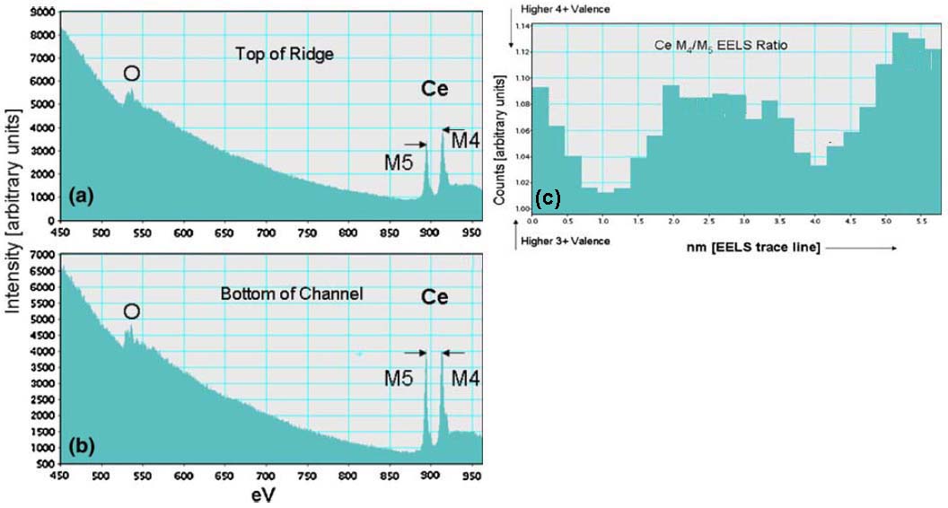
| In general, EELS spectra of cerium in materials display two sharp and strong features at 883 and 901 eV corresponding to the cerium M5 edge and M4 edge, respectively. Figure 2315a (a) and (b) shows EELS of ceria taken at two different locations of 3D (three-dimensional) ridge-valley structure of a Pt-ceria catalyst. The characteristic peak height inversion and edge splitting present normally oxidation state [1], indicating that a tall M4 edge is due to +4 valence and a tall M5 edge signals the presence of significant +3 valence. Therefore, the M4/M5 EELS ratio provides a good indication for both reduction potential and valence state. As an example, in Figure 2315a (c) the EELS M4/M5 ratio extracted from a line scan across the 3D catalyst indicates the variation of Ce valence across the material and the degree of Ce oxidation.
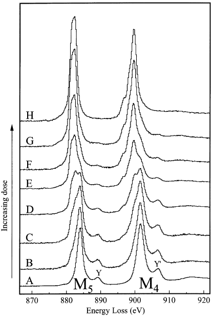
In some cases, the beam damage of the specimens in TEM measurements can be monitored by observation of energy-loss near-edge structure (ELNES), for instance, in the damage process of CeO2 specimens. The electron beam damage induces the changes in the spectral shape of a CeO2 specimen in thickness of 0.17λ within a few seconds. λ is inelastic mean free path. Figure 2315b shows the damage sequence from fresh CeO2 (A) to damaged CeO2 (H) with such thickness. After H, the edge showed no further changes with increase of electron dose. The M5 and M4 maxima and the peaks Y and Y' are associated with Ce4+. The electron-beam damaged CeO2 presents Ce M4,5 and O K-edge shapes that are consistent with reduction to a Ce3+ oxide. During the beam-damage process the spectrum of CeO2 changes as below:
Figure 2315b. The damage sequence from fresh CeO2 (A) to damaged CeO2 (H) in thickness of 0.17λ. The estimated doses in each case are (A) 3 x 10⁵ e/Å2; (B) 6 x 10⁵ e/Å2; (C) 2 x 10⁶ e/Å2; (D) 3 x 10⁶ e/Å2; (E) 7 x 10⁶ e/Å2; (F) 1 x 10⁷ e/Å2; (G) 2 x 10⁷ e/Å2; and (H) 5 x 10⁷ e/Å2. [3]
|