Chapter/Index: Introduction | A | B | C | D | E | F | G | H | I | J | K | L | M | N | O | P | Q | R | S | T | U | V | W | X | Y | Z | Appendix
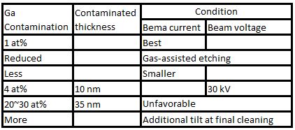
| Under unfavorable conditions, Ga (gallium) concentration at FIB prepared surfaces can be as high as 20 at% with a maximum depth of about 35 nm. For smaller ion beam currents, commonly used for the final cleaning, the Ga contamination is smaller. Significant amounts of Ga (up to ~ 30 at%) may build up in the redeposition layer, while the presence of Ga can be less than 1% in the amorphization region in many cases. The Ga concentration in the first 10-nm Si layer within the milled sidewalls was 4 at% when a 30 kV ion beam was used. [1] Ga can also accumulate at grain boundaries of milled surfaces, e.g. of aluminum (Al). Furthermore, GAE (gas-assisted etching) in FIB milling can significantly reduce the redeposition artifacts, and thus reduce Ga contamination. On the other hand, the materials deposited in FIB normally contain impurities. For instance, FIB-deposited tungsten material can consist of approximately 80% W, 5% O, 5% C, and 10% Ga if W(CO)6 precursor and Ga beam are used. Note that EDS analysis has been widely used to measure the gallium (Ga) concentration in materials, for instance, it has been applied to measure the Ga contamination in FIB-prepared TEM and SEM specimens even though EELS system has been installed in the same TEM systems. Table 2549 summarizes gallium contamination depending on FIB milling condition. Table 2549. Gallium contamination depending on FIB milling condition.
[1] T. Ishitani, H. Koike, T. Yaguchi, and T. Kamino, Implanted gallium-ion concentrations of focused-ion-beam prepared cross sections, J. Vac. Sci. Technol. B16, 1907 (1998).
|