Chapter/Index: Introduction | A | B | C | D | E | F | G | H | I | J | K | L | M | N | O | P | Q | R | S | T | U | V | W | X | Y | Z | Appendix
| The inelastical phonon excitation of incident electrons is also known as thermal diffuse scattering (TDS). Only electrons scattered at small angles and without loosing energies will contribute to the information in the HRTEM images while all the others (which have lost energy and have been scattered multiple times or at high angles) also contains important information about the sample, they will for instance give a diffuse background in the TEM images and benefit to EFTEM elemental mapping and EELS measurements. TDS electrons in Scanning Transmission Electron Microscopy (STEM) imaging refer to electrons that are scattered by phonons (vibrational modes) within the sample. This scattering is "incoherent" because it involves random interactions with the thermal vibrations of the atomic lattice rather than the ordered, periodic structure:
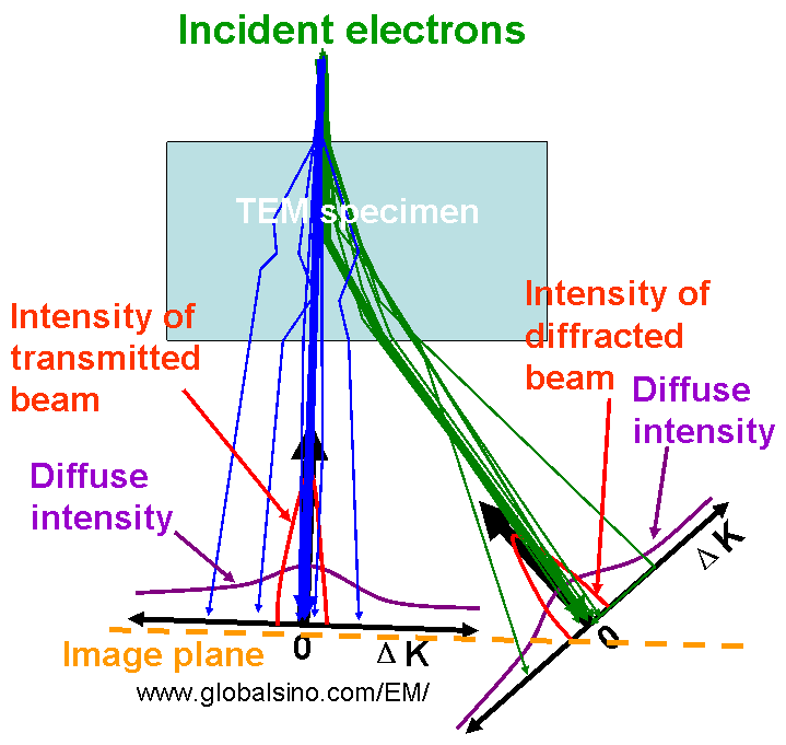
In TEM imaging, bright-field pictures are usually obtained at smaller angles and consist of a mixture of elastic, thermal diffuse, and inelastic scattering. When sample thickness exceeds few inelastic mean free paths (e.g. few hundreds of nanometers), the contribution of inelastic scattering dominates. Dark-field images are constructed using electrons scattered at relatively large (≥ 30 mrad for STEM) angles and are dominated by elastic and thermal diffuse scattering. Diffuse scattering (also called thermal diffuse scattering, TDS) is generated by the interaction of the probe electrons with pre-existing phonons in an EM specimen. TDS can also be described by elastic scattering modified by the atomic vibrations. TDS background in TEM measurements originates from both incoherent elastic and inelastic electron scatterings. Figure 4127a shows a schematic illustration of the process of incoherent inelastic scattering causing a diffuse background, generated by the transmitted beam and a diffraction beam. The energy and momentum transfers due to inelastic scattering are small. Randomly thermal vibration of atoms is also an important source of diffuse background. The overall diffuse effect reduces the constructive interference responsible for Bragg peaks. The diffuse background increases with TEM specimen thickness and beam intensity. For instance, the transmitted beam produces a higher background than the diffracted beams. Note that different from Bragg peaks, the diffuse scattering intensities are originated from local/temporal deviation from the long-range ordered structure.
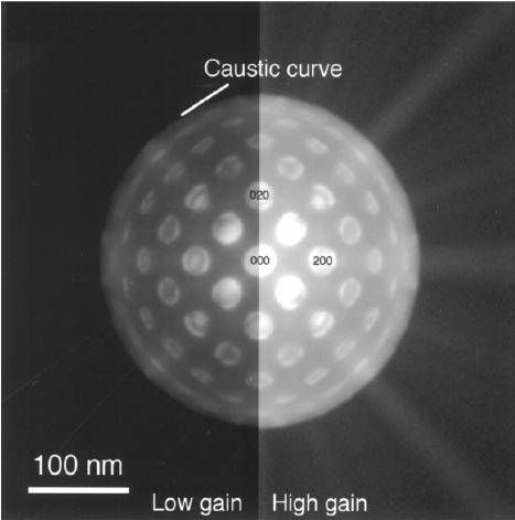
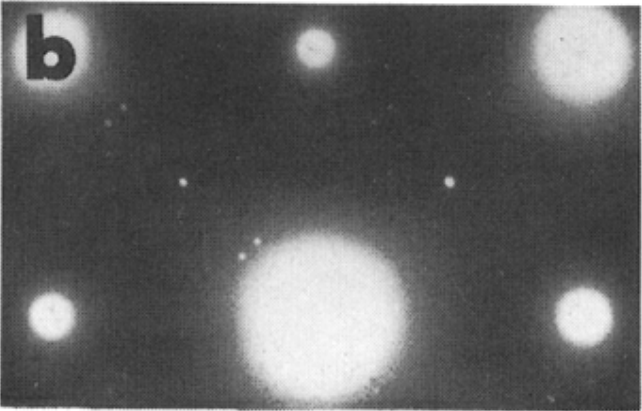
Diffuse scattering induced by thermal vibrations can be treated as electron–phonon scattering using a Debye phonon model [1 - 2]. Thermal diffuse scattering tends to occur through high-angles and thus those electrons are scattered beyond the objective apertures that are normally used in bright-field TEM imaging. Without an aperture, the contribution of TDS to the image is significant. In particular, high-angle incoherently scattered TDS electrons are subject to significant phase shifts from the rapidly varying portion of the lens transfer function and thus will extremely contribute a constant background to the image [4]. Incoherent electron scattering (not in phase) can be induced in uncorrelated scattering events from different scattering centers, for instance high angle elastic scattering or the inelastic scatterings. Figure 4127b shows an underfocus TEM image of a (001) SrTiO3 crystal with an incident probe focused on the specimen. The caustic curve is also indicated in the figure. High-angle thermal diffuse scattering is observed as Kikuchi bands, yielding background and a caustic curve.
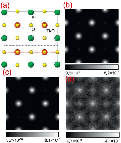
Although Figure 4127b appears to be convergent-beam electron diffraction patterns, it is TEM images at a magnification of 1E5 with a defocus of about +5 µm. Based on multislice simulation on SrTiO3 crystal structure (Figure 4127c (a)), Forbes et al. obtained the exit surface intensities with the total electron intensity, the elastically scattered electron intensity and the thermally scattered electron intensity. The simulation was carried out on a TEM specimen in thickness of 30 nm with a 300 keV electron probe.
Table 4127. Some details on diffuse spots or streaks.
[1] P. Rez, C. J. Humphreys and M. J. Whelan: “The distribution of intensity in
electron diffraction patterns due to phonon scattering.” Philos. Mag. 35, 81–86
(1977).
|