Chapter/Index: Introduction | A | B | C | D | E | F | G | H | I | J | K | L | M | N | O | P | Q | R | S | T | U | V | W | X | Y | Z | Appendix
| When an electron beam irradiates a target or specimen, most electron interactions with atoms result in energy losses (a few eV) as heat generated in the irradiated material, giving rise to a local temperature T that is higher than the temperature T0 of the surroundings as shown in Figure 4685a. For TEM observations, the heat deposited in the thin TEM specimen per second is given by, ΔQ = ΔE·(I/e) ·(t/λ) -------------------- [4685a] Where, The units of ΔQ is eV rather than Joule because the units of ΔE is eV. At the steady state of TEM imaging or elemental mapping, heat generation can be quickly balanced by heat loss due to radial thermal conduction and radiation in the vacuum. Therefore, we can have, I·ΔE·(t/λ) = 4πkt (T-T0)/[0.58 + 2ln(2R0/d)] + π(d2/2)εσ(T4-T40) ---------- [4685b] where,
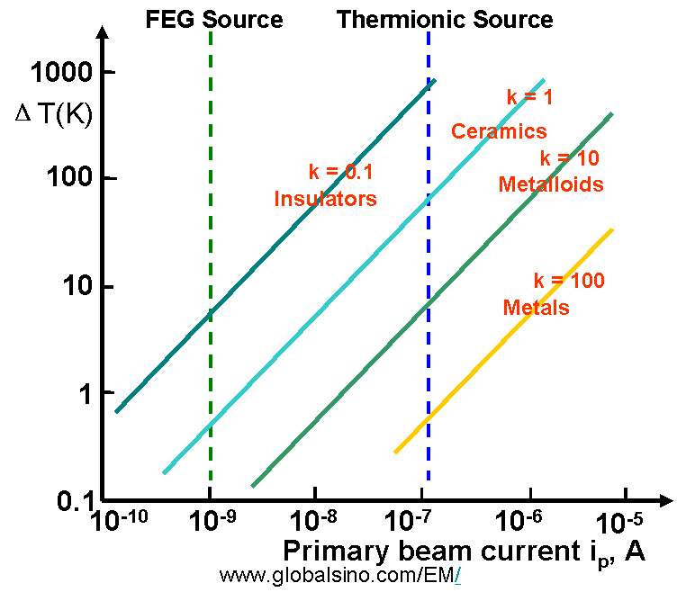
The first term on the right side of Equation 4685b represents the heat loss due to radial conduction over a distance R0 through the TEM film, while the second term the heat loss due to the radiation from both surfaces of the TEM specimen. Note that the radiation term (second term) is generally neglected in vacuum. Therefore, Equation 4685b becomes, I·ΔE·(t/λ) = 4πkt (T-T0)/[0.58 + 2ln(2R0/d)] ------------------------- [4685c] Figure 4685b shows the increase of TEM specimen temperature as a function of the electron beam current and the thermal conductivity k, in W·m-1K-1 of the specimen. Typical materials are also noted, but should not be considered representative because of substantial variation of k in any class of materials.
Figure 4685b. The increase of specimen temperature as a function of the electron beam current Figure 4685b indicates that beam heating in TEM is a problem at high incident currents, e.g. with a large or without condenser-lens aperture. But even at low current densities, heating effect is still a problem for insulators, such as polymers and other organic materials due to low k and low melting point. In EELS measurements on metal nano-structures, although the melting point of the metal nano-structures decreases dramatically with decrease of the structure size, it is unlikely, given a short acquisition time, that heating by the electron beam is an important factor causing specimen damage. The STEM probe is not expected to sufficiently increase the temperature of the metal enough to melt the surfaces of the nano-structures. On the other hand, although very small electron probes may induce a high current density, the temperature rise is usually insignificant as a result of the logarithmic term in Equation 4685c. For SEM observations, the specimen is normally a bulk material so that the heat flow is radial in three dimensions (3D), leading to a smaller temperature rise (typically from < 0.5 °C to a couple of degrees). Theoretically, when the probe size is much less than the electron range (R), the temperature rise in a stationary probe is given by [1], ΔT = (1.5/π) (IV0)/(kR) ------------------------- [4685d] Where, If the specimen is incorrectly mounted and/or thermal contact to the specimen holder is poor, the temperature can increase by tens of degrees. Phonons formed by the electron beam in EMs are essentially responsible for heating the specimen. However, because little information can be deduced from their intensity or angular distribution the formed phonons are rarely useful for detection in EMs.
[1] Reimer, L., 1998. Scanning ElectronMicroscopy, second ed, Springer, Berlin, pp. 118.
|