Chapter/Index: Introduction | A | B | C | D | E | F | G | H | I | J | K | L | M | N | O | P | Q | R | S | T | U | V | W | X | Y | Z | Appendix
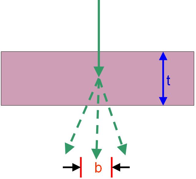
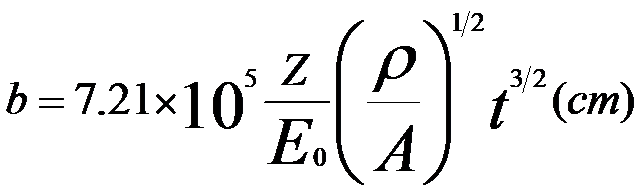
| Electron beam broadening (also called spreading) in an EM specimen is a phenomenon that the electrons from the incident beam distribute wider than the beam size due to scattering by the atoms in the irradiated materials. When the analysis electron probe is a few nanometers in diameter, beam broadening within the specimen plays a critical role in affecting the spatial resolution. Electron beam broadening affects especially the spatial resolution of the techniques based on small electron beams, for instance, in EDS technique and TEM imaging. Beam broadening in a thick specimen is difficult to calculate because multiple scattering is involved. In this case, e.g. ≥80 nm for Si, the surface-plasmon effects becomes negligible, while the beam spreading becomes significant because more electrons suffer inelastic collision in larger scattering angles. More electrons scatter outside the finite collection aperture. The first model of beam broadening in a thin film was developed by Reed [1], who assumed that a single, Rutherford scattering event occurred at the centre of the foil, and in X-ray measurements he defined the broadened size of X-ray source as that volume in which 90% of the electron trajectories lay as shown in Figure 4626. Electron beam broadening in a thin film, e.g. a TEM or STEM specimen, can be calculated by the “single-scattering” model that assumes each electron is only scattered once when traveling through the very thin specimen. In this case, the thin specimens act as weak phase objects so that the extent of beam broadening (b) caused by elastic scattering can be given by, For instance, at 100 keV of an incident electron beam, a 100 nm thick specimen presents a beam broadening of the order of 10 nm. For a Gaussian probe, the average interaction size, D, through the TEM film, is given by, In CBED measurements, the size of the region where the electron beam interacts is limited only by the beam size and the beam-specimen interaction volume. As indicated in Equation 4626a, determination of the beam broadening within the specimen requires the knowledge of the specimen thickness. There are some techniques which can be used to measure the specimen thickness.
Figure 4626. First model of beam broadening in a thin film. Some researchers have theoretically studied beam broadening in thin films based on Monte Carlo techniques[2, 3], which agree well with the simple model of Reed up to thicknesses of a few mean free paths. Some researchers have also employed experimental measurements to examine beam broadening on materials, such as augite lamellae in an orthopyroxene [4], Fe-Ni alloys [5], gold [6], and chromium [6]. For a typical sample thickness (100 nm), the beam broadening for rutile is about 8.5 nm at 200 keV incident beam energy. In principle, the beam broadening is weaker for thinner samples. Based on Equation 4626a, the spatial resolution for both the EDS and EELS analyses is improved with the accelerating voltages, since the incident electron beam spread decreases with an increase in the accelerating voltage. On the other hand, based on Equations 4626a and 4626b, to minimize D, one also need to use as thin a specimen and as small a probe diameter as possible.
[1] Goldstein, J. I., Costley, J. L., Lorimer, G. W., and Reed,
S. J. B. (1977) SEM 1977 (O. Johari, ed.) Pub. 11RT1,
Chicago, 315.
|
 --------------------------- [4626a]
 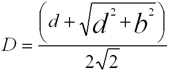 --------------------------- [4626b]