=================================================================================
Silicon drift detectors (SDDs) are a type of X-ray radiation detectors and have been widely applied to perform electron microscopy (SEM/STEM)-EDS and X-ray fluorescence analysis (XRF) in high resolution and with high count rate. On the other hand, due to high purity silicon (Si) used, a low level of leakage current facilitates operations close to room temperature with moderate (Peltier) cooling instead of the traditional liquid nitrogen.
Gatti & Rehak [1] proposed a basic structure of silicon drift detector in 1983. Table 2528 lists the detailed development history of silicon drift detectors.
There are mainly two types of silicon drift detectors:
i) Based on concentric rings.
This type of SDDs allows large areas with good resolution.
ii) Based on droplet rings.
This type of SDDs hides the pickup and FET (field effect transistor) under the collimator.
The FETs can be either discreet or integrated on the detector crystal. The discreet FETs have the advantage of lower noise potential in FETs, but the manufacturing process is complex and the device is sensitive to microphonics. On the other hand, the integrated FETs provide higher count rates due to lower capacitance.
As an example, Figure 2532a shows the schematic illustration of SDDs based on concentric rings. This device is composed of a volume of fully depleted highly-resistive silicon, in which a strong electric transversal field (parallel to the surface) drives the X-ray-generated-electrons towards a small collection anode. This transversal field is induced by a number of increasingly reverse biased strips (ring electrodes), and causes charge carriers to 'drift' to the collection electrode. The collection electrode together with the integrated FET converts the current into a voltage. The radiation entrance window on the opposite side is made up by a non-structured shallow implanted junction, resulting in a homogeneous sensitivity over the entire detector area. In this way, similar to other solid state X-ray detectors, SDDs measure the energies of the incoming X-rays by the amount of ionization produced in the detector material.
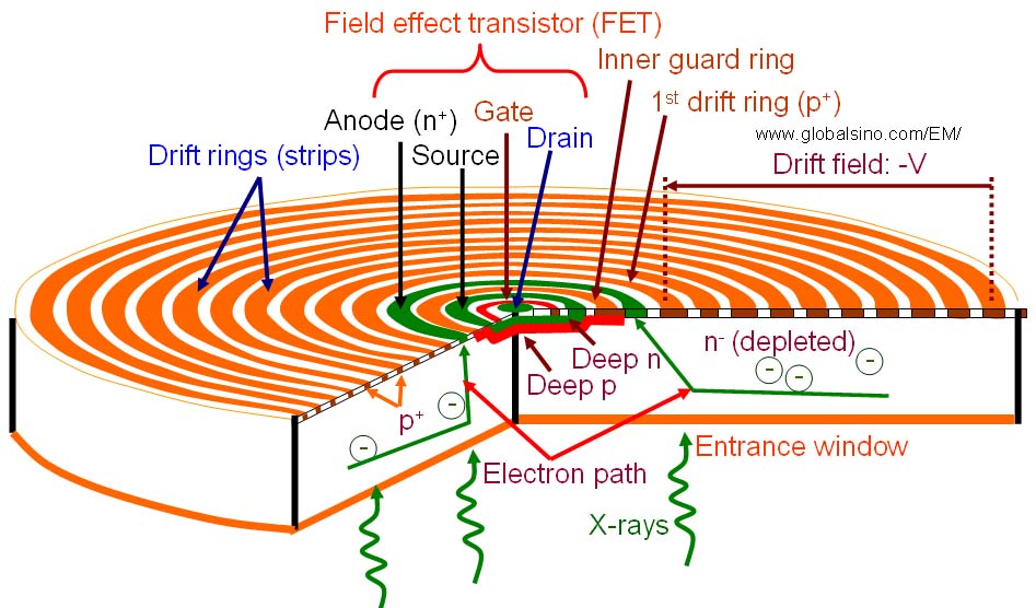
Figure 2532a. Schematic illustration of silicon drift detector (SDD) for X-ray spectroscopy.
Figure 2532b shows an example of a typical silicon drift detector which is a Bruker Round 30 mm2 SDD with Al contact on the entrance window.
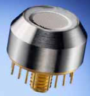
Figure 2532b. Example of a typical silicon drift detector.
Figure 2532c shows the comparison between the detection efficiencies of Si(Li) and SDD detectors. Si(Li) detectors are more sensitive to high-energy x-rays because of the greater thickness of the Si(Li) sensors, while the SDD detectors are less sensitive because the high-energy X-rays easily penetrates through the “thinner” SDD sensor.
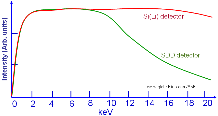
Figure 2532c. The comparison between the detection efficiencies of Si(Li) and SDD detectors.
Figure 2532d shows the schematic illustration of an EDS system integrated with a SDD chip.
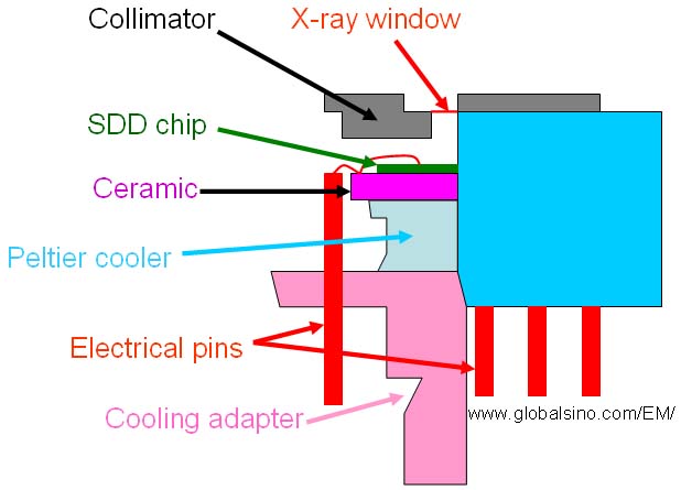
Figure 2532d. Schematic illustration of an EDS system integrated with a SDD chip.
Furthermore, page2527 lists the comparison of various X-ray spectrometers, including lithium-drifted silicon (Si(Li)), Si-drift detectors (SDD), intrinsic-Ge (IG), wavelength dispersive X-ray spectroscopy (WDXRF/WDS), and Bolometer detectors.
[1] E. Gatti, P. Rehak, Semiconductor Drift Chamber - An Application of a Novel Charge Transport Scheme, Nucl. Instr. and Meth. A 225, 1984, pp. 608-614.
|