Chapter/Index: Introduction | A | B | C | D | E | F | G | H | I | J | K | L | M | N | O | P | Q | R | S | T | U | V | W | X | Y | Z | Appendix
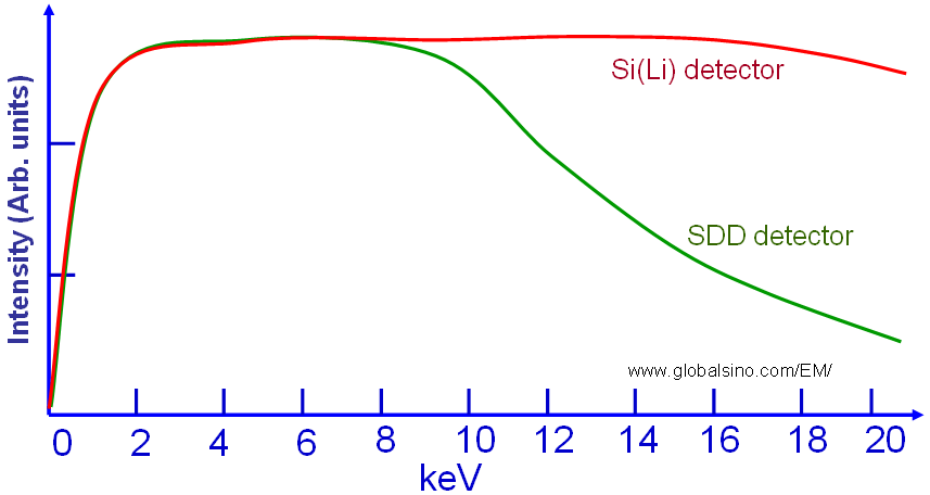
| Application of low energy X-rays for EDS analysis is limited by the absorption in the carbonaceous contamination layer on the specimen surface and the ice layer on the detector crystal. There are many drawbacks induced by such effects, for instance: In EDS measurements, the path of X-ray absorption mainly depends on two factors: High take-off angles decrease absorption of the X-rays, while low take-off angles increase absorption because the X-rays must penetrate more material. X-ray absorption increases rapidly for take-off angles under 25°, but is relatively constant for angles greater than 35°. Note that the Kramers' algorithm presents a relatively poor approximation of the actual spectrum because it does not involve the X-ray absorption in the specimens, which is wavelength dependent and attenuate the longer wavelengths to a far greater degree than the shorter wavelengths. Furthermore, in general, absorption corrections are always required for the light-element X-rays. The EDS detection of low-energy X-rays is limited by X-ray absorption as indicated in Figure 2538.
Figure 2538. Comparison between the detection efficiencies of Si(Li) and SDD detectors. For SEM-EDS measurements on bulk materials, beam energy of 20 keV is a good compromise between both the requirements of obtaining adequate overvoltages and of minimizing absorption in the specimen. However, such beam energy may still mask the presence of light elements that only produce X-ray energies below 2 keV since their high overvoltage (e.g. U >10) will lead to deep penetration of the incident electrons into the specimen, and thus the absorption can be as high as 50-99%. To avoid missing possible light elements present at low concentrations, spectrum acquisitions should be repeated at beam energies in the range of 5-10 keV. In a sufficiently thin TEM specimen, the incident beam looses only a small amount of energy and the ionization cross-section is constant along the electron path. To a first approximation, X-ray absorption and secondary X-ray fluorescence within the specimen can normally be ignored. However, comparing with SEM-EDS method, TEM specimens can still be used to simplify EDS measurements, especially quantifications, as the thin specimens avoid significant x-ray absorption and secondary x-ray fluorescence events. Those two factors typically cause significant EDS inaccuracy with bulk specimens in an electron beam microprobe or a scanning electron microscope. In this case, the main advantage of using a thin specimen for x-ray microanalysis are: Note that contaminants on TEM specimen surfaces also limit a number of applications, e.g. low energy EDS analysis and EELS analysis. When there are no significant differences in their X-ray absorption coefficients for the elements in the specimen, or when the specimen is thin enough, X-ray absorption corrections may be neglected to obtain an accuracy of 10-20%. However, to obtain an accuracy in the range of 5-10%, an absorption correction should be applied with an estimate of the specimen thickness.
|