Chapter/Index: Introduction | A | B | C | D | E | F | G | H | I | J | K | L | M | N | O | P | Q | R | S | T | U | V | W | X | Y | Z | Appendix
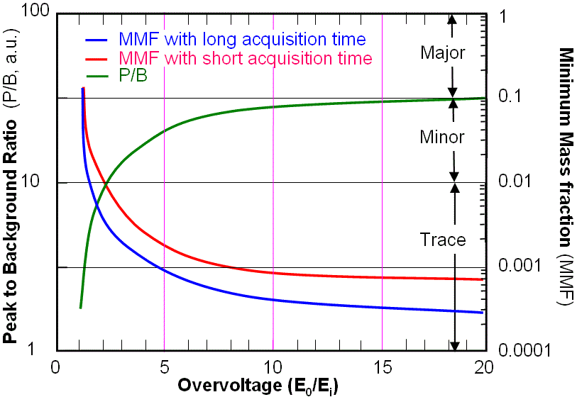
Overvoltage ratio (or simply called overvoltage) is the ratio of the beam energy E0 to the ionization energy Ei, which is E0/Ei. Here Ei is the ionization energy of a given element in the K-, L-, or M-shells (keV) and E0 is the accelerating voltage of the electron microscope. This concept is used for evaluating the ionization cross section. Therefore, in elemental quantification based on EDS measurements, the setting of the overvoltage on EDS software may strongly affect the ionization cross section. For EDS measurements on bulk specimens in SEMs, it is necessary to select an optimum overvoltage for a specific X-ray line. In general, Figure 4612 shows the behavior of peak-to-background ratio and minimum mass fraction (detection limit) as a function of overvoltage. It is important that X-ray yields, at low energy of incident electrons, depend strongly on overvoltage (especially when U<3) since too small overvoltage would lead to less efficiency of X-ray excitation. In order to be able to detect minor elements, the overvoltage must be not less than 2, while bigger overvoltage and/or longer acquisition time should be used if the detection of trace elements is needed. However, too high overvoltage would unnecessarily degrade spatial resolution and cause greater X-ray absorption because the X-rays are generated deeper in the specimen. In this SEM-EDS measurements on bulk materials, beam energy of 20 keV is a good compromise between both the requirements of obtaining adequate overvoltages and of minimizing absorption in the specimen. However, such beam energy may still mask the presence of light elements that only produce X-ray energies below 2 keV since their high overvoltage (e.g. U >10) will lead to deep penetration of the incident electrons into the specimen, and thus the absorption can be as high as 50-99%. For optimized SEM-EDS measurements, the typical overvoltage should be at least 2 for the highest energy line and no more than 20 for the lowest energy line of interest since the absorption affects more on low X-ray energy lines. Furthermore, to avoid missing possible light elements present at low concentrations, spectrum acquisitions should be repeated at beam energies in the range of 5-10 keV.
For effective generation of X-ray by ionization processed by electron interaction, the overvoltage U should be greater than 1.3 because the X-ray peak to background ratio (P/B) of X-ray signal is reduced substantially as E0 (energy of incident beam) approaches Ei (ionization energy). It is necessary to mention that the low energy X-ray lines, e.g. Cu(L) at 0.93 keV instead of Cu(K) at 8.04 keV, are used at low accelerating voltage of incident electrons. Applicable X-ray lines to identify the elements from beryllium to uranium are in the energy range of 0.1 keV to 20 keV. In order to provide a proper over-voltage to excite the X-ray lines in the upper half of this range, the energy of the incident electron beam should be in the range 20-30 keV. For EDS measurements on thin-film specimens in STEMs and TEMs, it is not necessary to use small overvoltages since X-ray absorption is not a problem. |
|
|
|