Chapter/Index: Introduction | A | B | C | D | E | F | G | H | I | J | K | L | M | N | O | P | Q | R | S | T | U | V | W | X | Y | Z | Appendix
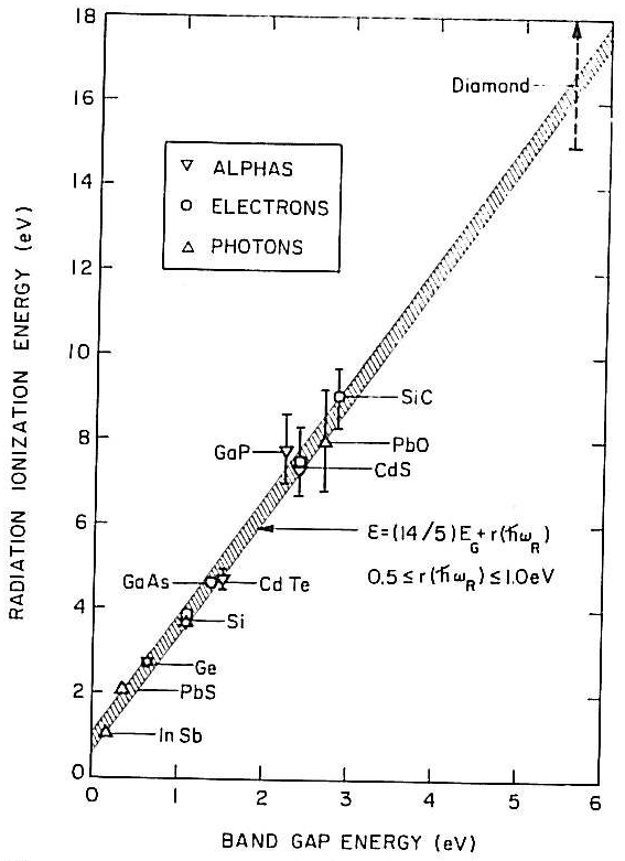
| Generally EELS (Electron Energy Loss Spectroscopy) has better sensitivity than EDS (Energy-dispersive X-ray spectroscopy), due to the potential of utilizing signals generated from larger ionization cross sections (L rather than K) and the much greater collection efficiency. [1 - 2] The X-ray photons carrying the elemental information propagate along all directions in space. However, it is difficult to insert a large detector in an electron beam column without affecting other capabilities of the TEM and X-rays cannot be deflected into an appropriate detector so that their collection is always inefficient (usually between 1 and 3 %) and thus signal intensity is a problem from a thin specimen. The EDS detector is highly efficient for the detection of some elements, for instance, it is almost 100% efficient for the detection of Fe Kα X-ray, while for Si Kα x-ray the detection efficiency is significantly degraded due to x-ray absorption in the detector itself. Furthermore, the general detection efficiency of the X-ray spectrometer falls rapidly below ~1 keV. The X-ray collection efficiency in EDS measurements is determined by the geometry between the sample and detector. Two main factors that affect the number of X-ray photons which reach the detector are: The geometric collection efficiency, referring to the solid angle of spectrometer acceptance, can be given by (Ω/4π) x 100%. For the TEM configuration with a top-entry type EDS detector, the detector is placed above the objective lens in a TEM system with a high viewing angle (e.g. 70 °) to a horizontal specimen. Since X-rays entering the detector take a large take-off angle (TOA) against the specimen, a high accuracy of quantitative analysis can be obtained. However, with such configuration, the solid angle of the detector against the specimen is small, resulting in low detection efficiency. For TEMs with top-entry stages, it is impossible to get X-ray detectors near the specimen in EDS analysis so that analytical microscopy is very inefficient. The X-ray collection efficiency of ultra-thin window (UTW) EDS detectors is decreased because the EDS detectors cannot be positioned close to the specimen due to the airlock mechanism and the magnetic electron trap. In modern EMs, Windowless in-column silicon drift detectors have been installed, which provides very high collection angle (e.g. 0.9 sr) and thus, allows high detection efficiency (e.g. 7% of the x-rays emitted from the EM specimen). Figure 4789a and table 4789 shows the average energy required to form one electron-hole pair versus bandgap energy for a number of semiconductor materials.
Figure 4789a. The average energy required to form one electron-hole pair versus Table 4789. Properties of Semiconductor Materials. [3]
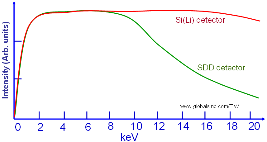
Because of electron beam damage, especially in the measurements with field emission guns, S/TEM microanalysis needs not only high count rate capability but also high collection efficiency of the X-rays in order to reduce the dose on the specimen in EDS measurements. In the x-ray detection, the emitted x-rays of element A (IEA) from an EM specimen are attenuated by the Be (beryllium) window and the Au (gold) contact layer on the detector surface and the Si dead layer of the detector itself. Therefore, the detected x-ray intensity of element A, IA, can be given by, where, The manufacturers of EDS systems should be able to provide the numbers about the thicknesses of Be window, Au film, and the dead layer in the detector. Note that the k factors for light (smaller Z) elements (low energy X-rays) normally are strongly affected by those detector parameters mentioned above. Furthermore, Figure 4789b shows the comparison between the detection efficiencies of Si(Li) and SDD detectors. Si(Li) detectors are more sensitive to high-energy x-rays because of the greater thickness of the Si(Li) sensors, while the SDD detectors are less sensitive because the high-energy X-rays easily penetrates through the “thinner” SDD sensor. In general, the EDS detection of low-energy X-rays is mainly limited by X-ray absorption, the detection of high-energy X-rays is mainly limited because the detector becomes transparent.
Figure 4789b. The comparison between the detection efficiencies of Si(Li) and SDD detectors. Overall, the efficiency of an EDS detector is mainly affected by the following factors:
[1] M. Isaacson, D. Johnson, Ultramicroscopy 1 (1975) 33.
|
 -- [4789b]