=================================================================================
The Si L2,3 signal yields a much higher signal-to-noise ratio (SNR) than the Si K edge. In EELS analysis, the main edges which are used in Si characterization are Si L2,3 edge ( L3 99 eV and L2 100 eV) and Si K edge (1839 eV) as shown in Figure 3441a.
|
(a) |
|
(b) |
| Figure 3441a. Main edges (after removed background) used in Si characterization: (a) Si L2,3 edge ( L3 99 eV and L2 100 eV) obtained with energy dispersion of 0.5 eV/channel
, and (b) Si K edge (1839 eV). |
|
It is necessary to note that the Al L2,3 edge and Si L2,3 edge in EEL spectra are very close as shown in Figure 3441b.
|
| Figure 3441b. Al L2,3 edge ( L3 73 eV and L2 74 eV) and Si L2,3 edge ( L3 99 eV and L2 100 eV) in EELS. |
|
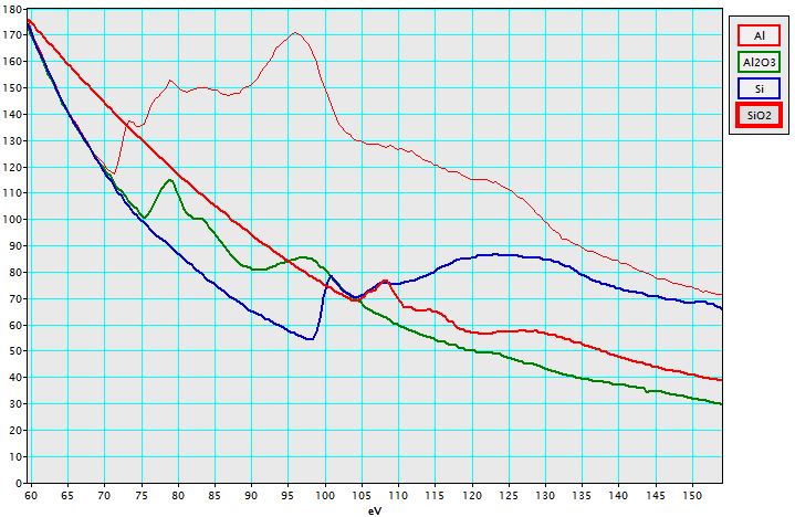
The EEL spectra in Figure 3441c show the Al L2,3 edge as well as the Si L2,3 edge after background subtraction, taken from AlxSiyOz matrix. The threshold value of the Al ionization edge here is about 75 eV indicating that aluminum is bonded to oxygen because the onset energy of the edge of pure aluminum is about 73 eV. This energy difference is called chemical shift. Depending on the environment of Si element, the chemical shift of Si L2,3 energy loss edge can be up to 6.9 eV.
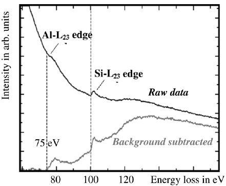
Figure 3441c. EELS profile of Al and Si taken from AlxSiyOz matrix by a electron probe of 2 nm in diameter. [1]
Many Si-based materials, e.g. some minerals, consist of SiO4 tetrahedron. These tetrahedra may form crystalline silica polymorphs, as well as amorphous and glassy phases. In Figure 3441d, the Si L2,3 edges from quartz and the two clay minerals shows very similar edge shapes, characterized by two sharp peaks, i.e. peaks A (106.3 eV) and B (108.4 eV), followed by a sharp peak C (115.0 eV) and a broad peak D (133 eV). Peak A, from quartz, is further split into two peaks separated by 0.45 eV.
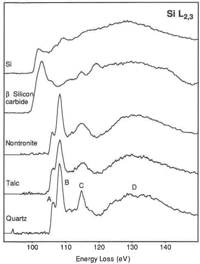
Figure 3441d. Si L2,3 edges from three silicates containing SiO4 tetrahedra
(qtartz, talc, and nontronite), as well as from β-SiC and pure Si.
[2]
The resulting chemical shift can be mapped using the energy filtered imaging taken with a narrow energy slit of 1.8 eV or similar spectrum mapping in STEM mode.
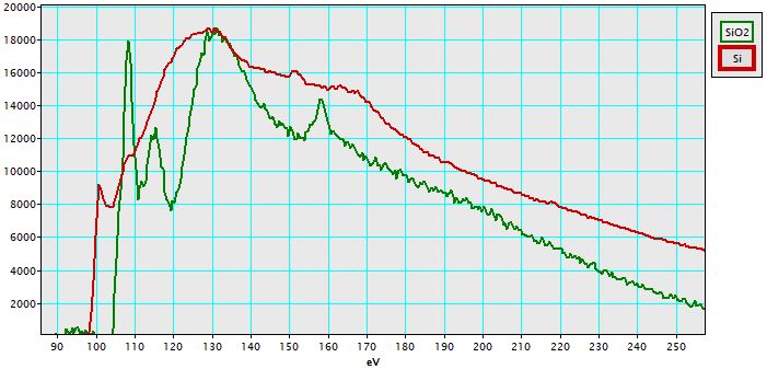
The silicon ‘metallic’ bulk plasmon is found at 17 eV, and it moves up to 23 eV for silicon nitride (Si3N4). Figure 3441e shows the Si L2,3 EEL spectra of Si, SiO2 and Si3N4. The positions of the edge onsets clearly indicate chemical shifts and differences in ELNES present. Table 3441a lists the Si L2,3 energy loss onsets (EL2,3) of some Si compounds and chemical shifts (ΔEL2,3) from that of pure Si. In Figure 3441e, for pure Si, the ELNES shows a first peak at 101.5 eV followed by a small plateau between 105 and 114 eV, and a very broad peak with the maximum at 135 eV. The SiO2 ELNES has a strong peak at 108.5 eV, which is also followed by a small plateau between 112 and 116 eV. However, the second peak located at 128 eV is far less intensive than the one for Si. An additional small peak presents at 161 eV. The ELNES of Si3N4 is very similar to the SiO2 ELNES. The two main peaks are located at 105 and 124.5 eV.
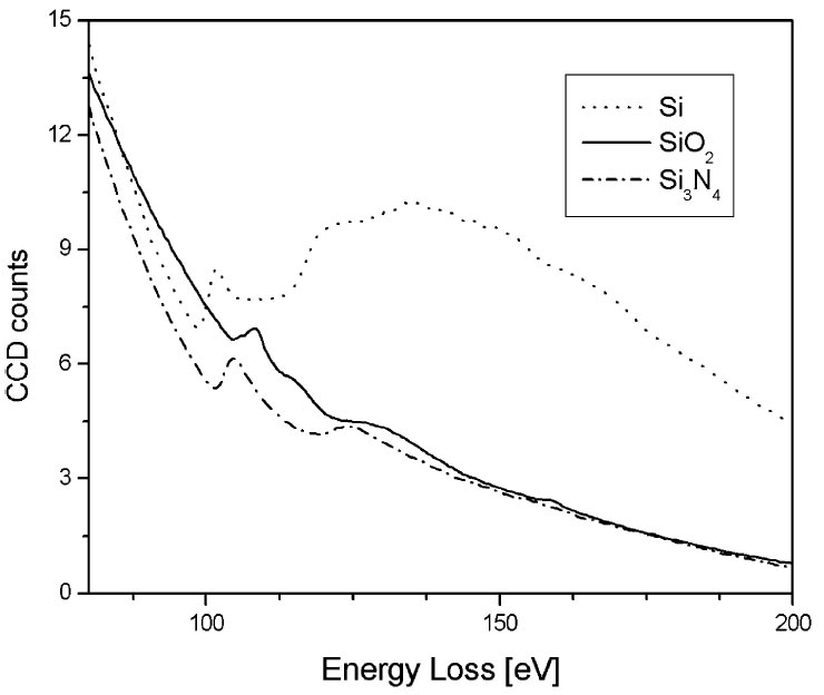
Figure 3441e. Si L2,3 EEL spectra of Si, SiO2 and Si3N4. [3]
Table 3441a. Si-L2,3, Si-L1, and Si-K energy loss onsets (EL2,3, EL1, and EK) of
some Si compounds and chemical shifts (ΔEL2,3, ΔEL1, ΔEK) from that of pure Si.
| Compound |
EL2,3, eV |
ΔEL2,3, eV |
EL1, eV |
ΔEL1, eV |
EK, eV |
ΔEK, eV |
| Si |
99.2 |
|
149.86 |
|
1839 |
|
| SiO2 |
105.3 |
6.1 |
|
5.7 |
|
7.2 |
| Si3N4 |
101.5 |
2.3 |
|
3.1 |
|
3.9 |
| CoSi |
100.6 |
1.4 |
|
|
|
|
| CoSi2 |
100.6 |
1.4 |
|
|
|
|
In order to distinguish different compounds containing a specific element, e.g. silicon in pure Si, SiO2 and Si3N4, the positions of the energy windows (in three-window method) and respective slit widths have to be chosen according to the ELNES as mentioned above. Table 3441b shows the optimized imaging filter settings in three-window EFTEM mode for Si, SiO2 and Si3N4. For Si mapping in SiO2 the post-edge window was placed above the second peak at 143 eV (See Table 3441b). The two pre-edge windows were placed in the small plateau region between the first (110 eV) and the second (125 eV) peaks. The optimal slit width was found to be 5 eV. The filter settings for Si3N4 were determined in a similar way by considering the shift of the Si L2,3 spectrum towards lower energy loss energies. Therefore the pre-edge windows were placed at 107 and 110 eV. The post-edge window was placed at 114 eV in order to avoid interference with Si and SiO2 signals. A slit width of 3 eV was used. Those settings were used to take Si images in a MOSFET structure as shown in Figure 3441f. Note that in those images, SiO2 and Si3N4 can be distinguished without mapping O and N elements. It is clearly shown that the polycrystalline Si gate (a) is separated by a thin dielectric layer (b) from the single crystalline Si (c). The spacers (d) consisting of two different types of material can be seen on both sides of the gate. Between the polycrystalline gate and the single crystalline Si, the gate oxide layer is also seen clearly. The spacers consist of two layers, namely a thin SiO2 layer and a thicker Si3N4 layer. Note that the bright contrast at the top of image (c) can be an artifact because of the signal of some elements overlapping the Si energy windows of SiO2.
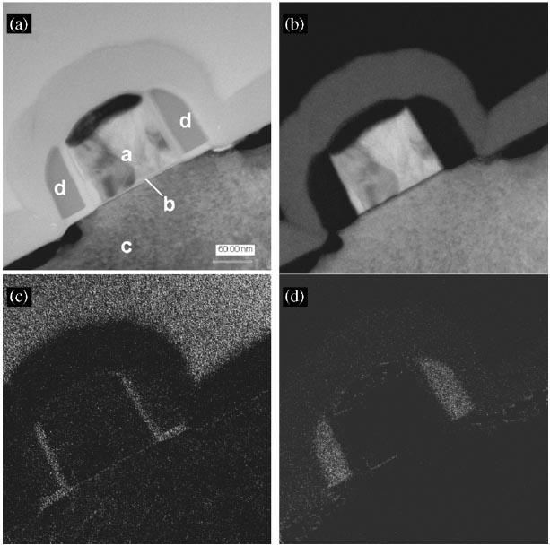
Figure 3441f. TEM bright field image and ELNES Si maps of the MOSFET structure: (a) TEM bright field image; (b) Si map; (c) Si map in SiO2; (d) Si map in Si3N4.
[3]
Table 3441b. The imaging filter settings of EFTEM for Si, SiO2 and Si3N4. [3]
| Compound |
Pre-edge window 1 (eV) |
Pre-edge window 2 (eV) |
Post-edge window (eV) |
Slit width (eV) |
Si |
73 |
87 |
119 |
20 |
SiO2 |
110 |
125 |
143 |
5 |
Si3N4 |
107 |
110 |
114 |
3 |
The valence state of Co can be indirectly determined by mapping the Si ELNES characteristics for the cases of CoSix (x = 1 or 2). Figure 3441g shows the as-measured and background-subtracted Si L2,3 EELS spectra of CoSi and CoSi2. The spectra for both silicides have Si L2,3 edge onsets located at 100.6 eV, while the Si ELNESs are slightly different. The CoSi2 ELNES has one broad peak with a characteristic pre-edge peak, while the CoSi ELNES does not show this pre-edge peak. Based on those characteristics, the parameters for three-window EFTEM method in Table 3441e are used. Here, in order to distinguish between CoSi and CoSi2, the pre-edge peak of CoSi2 was used, while the third peak of CoSi at 145 eV was used for the post-edge window. Using those settings, the Si ELNES maps of CoSi and CoSi2 were obtained together with TEM image as shown in Figure 3441h. Note that the Ti, Co, and Si elements have overlapped layers as indicated in Figure 3441h (a). Although the Ti film also gave some artefacts in the maps, it is very important that the grains consisting of CoSi and CoSi2 were still distinguished and the images revealed that a CoSi2 layer was formed between CoSi and Si substrate.
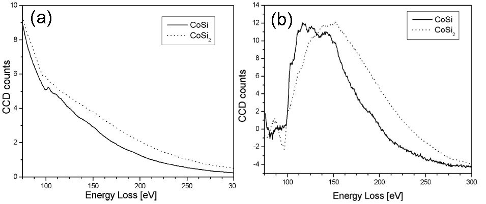
Figure 3441g. The as-measured (a), and background-subtracted (b) Si L2,3 EELS spectra of CoSi and CoSi2. Adapted from [3]
Table 3441c. Three-windows imaging filter settings for Si L2,3 ELNES for CoSi and CoSi2. [3]
| Compound |
Pre-edge window 1 (eV) |
Pre-edge window 2 (eV) |
Post-edge window (eV) |
Slit width (eV) |
CoSi |
125 |
130 |
145 |
10 |
CoSi2 |
67 |
77 |
91 |
6 |
Figure 3441h. The TEM image (a), CoSi map (b), and CoSi2 map (c) of Ti/CoSi/CoSi2 layer stack. Adapted from [3].
Figure 3441i shows that the chemical shifts are revealed by spatially resolved EELS of Si-L2,3 edges. Figure 3441i (a) shows the 2-D (two-dimensional) spectrum image obtained by an energy filter. Note that this image shows the image contrast before background subtraction. The vertical axis corresponds to the location (y) in the layered materials of SiON. Si3N4, SiO2 and pure Si. The horizontal axis corresponds to the energy loss E. Energy dispersion used here was 0.051 eV per pixel. The energy range ΔE recorded in the 2-D spectrum image was 52 eV (= 88 - 141 eV in energy loss). Both the shift of the bright lines (shown by red arrows) in Figure 3441i (a) and the vertical lines in Figure 3441i (b) indicate the chemical shift of Si-L2,3 edges. Figure 3441i (b) shows energy loss spectra of each layer extracted from Figure 3441i (a). Here, the backgrounds of the spectra were subtracted. It is necessary to point out that the spectra in Figure 3441e were not background-subtracted, while they were background-subtracted in Figure 3441i (b). Another difference of ELNES between the two “pure” Si spectra in Figure 3441e and 3441i (b) probably originated from the quality of the silicon materials or their impurities.
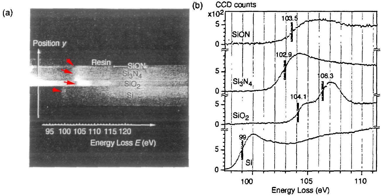
Figure 3441i. The spatially resolved EELS analysis of Si-L2,3 edges, (a) 2-D spectrum
image and (b) spectra of SiON. Si3N4, SiO2 and pure Si. Adapted from [4]
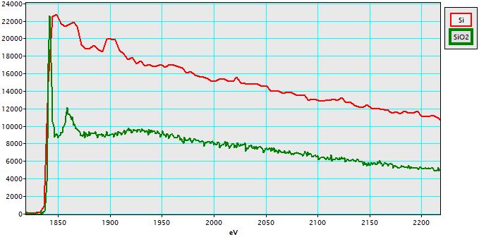
Figure 3441j shows the spatially resolved EELS of Si-K edges: (a) 2D spectrum image and (b) spectra of Si3N4, SiO2 and Si. Those spectra are about two orders of magnitude weaker than that of the L2,3 edges so that the experimental conditions are different. For instance, the energy dispersion for Si-K edges is decreased to 0.30 eV (0.051 eV for Si-L2,3 edge described above) per pixel.
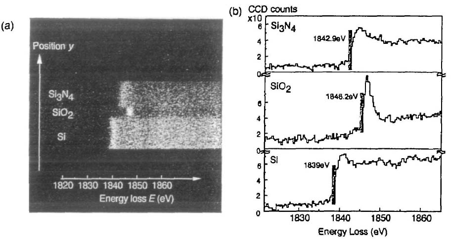
Figure 3441j. The spatially resolved EELS of Si-K edges: (a) 2D spectrum image and (b) spectra of Si3N4, SiO2 and Si. [4]
Figure 3441k shows the plasmon regions and Ni–M2,3 edges of the three nickel silicide phases in EELS. The three phases can be distinguished by their bulk plasmon energy position (Ep). The energy positions are shifted from 19.4 eV for NiSi2, to 20 eV for NiSi and 22.2 eV for Ni2Si. The Ni–M2,3 core edge shifts can also be obtained from 65.8 eV for Ni2Si and 66.8 eV for NiSi to 67.5 eV for NiSi2.
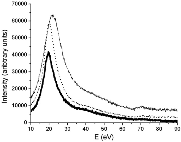
Figure 3441k. The plasmon regions and Ni–M2,3 edges of the three nickel silicide phases in EELS: The solid thin line represents Ni2Si, the dotted line NiSi and the thick solid line NiSi2.
[5]
Brown and Ho [6] used an EELS spectrometer with an incident electron energy of 10 eV, consisting of a double-pass cylindrical monochromator and single-pass cylindrical analyzer, to analyze the interaction between methyl chloride and Si( 100) 2 x 1. Figure 3441l shows the EEL spectra obtained after 1 L exposures of methyl chloride (CH3CI) onto the Si(100) surface held at 85 and 300 K. The origin of the peaks, related to the existence of molecularly adsorbed species, is listed in Table 3441f.
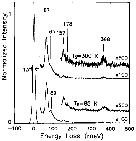
Figure 3441l. The EEL spectra obtained after 1 L exposures of methyl chloride onto the Si(100) surface held at 85 and 300 K. [6]
Table 3441d. The origin of the peaks in Figure 3441l.
| Energy loss |
Origin |
| 67 meV |
The Si-Cl stretch: an adsorbed chlorine atom |
| 89
meV |
The C-Cl stretch of a
weakly bound methyl chloride molecule |
| 85 meV |
The Si-(CH3) stretch |
| 157 meV |
The CH3 symmetric deformation mode |
| 178 meV |
The CH3 asymmetric deformation mode |
| 368 meV |
The C-H stretch
modes |
Figure 3441m shows experimental ELNES spectra at the Si-L2,3 edge taken from amorphous, C49, and C54 TiSi2. All the three spectra consist of a small peak located at around 102 eV superposed on a very broad peak. The clear difference between three spectra is the width of the first peak. This peak is sharper in the C54 sample than in the C49 sample, while the amorphous sample is similar to the C49 sample.
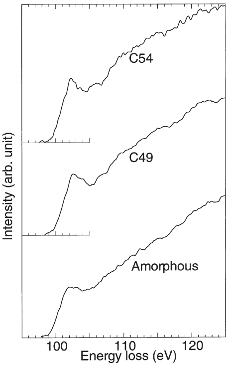
Figure 3441m. Experimental Si-L2,3 edge ELNES spectra taken from amorphous, C49, and C54 TiSi2.
[7]
In many cases, the deep level states in semiconductors can be analyzed by EELS measurements. For instance, the pronounced shoulder below 100 eV indicated by the arrow in Figure 3441n presents a deep level state, above Fermi level in band gap, produced by symmetric segment a 5-fold coordinated atom in CSL junction in polycrystalline silicon. The shoulder in the Si-L2,3 ELNES was detected only from the symmetric segment of the {112} Σ3 CSL boundary near the CSL junction, but not from the bulk, {112} and {111} Σ3 CSL boundaries. The CSL junction would be electrically active and affects the electrical conductivity in polycrystalline silicon.
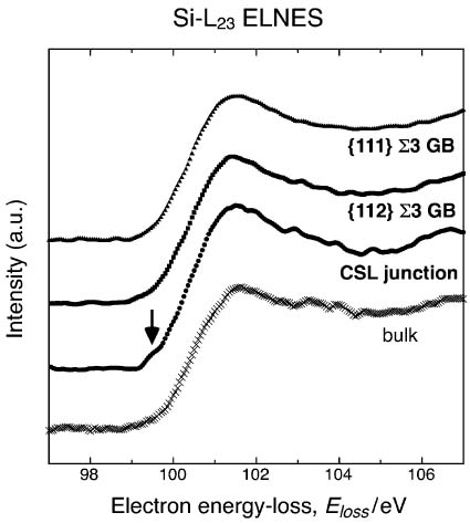
Figure 3441n. The energy-loss near-edge spectra (ELNES) of Si-L2,3 edge acquired from a bulk, {112} and {111} Σ3 CSL boundaries, and their junction.
[8]
Single scattering distribution (SSD) spectra can be extracted from experimental spectra by deconvolution of elastic/quasi-elastic phonon and multiple scattering effects. For instance, this deconvolution can be done by removing multiple scattering with Fourier-log deconvolution method. For some materials (especially wide band gap materials), the band gap (Eg) from low-loss spectra obtained by EELS technique can be determined by eye observation of the SSD spectrum. In this case, Eg is defined as the energy corresponding to the first onset in the spectrum, for instance, 0.67 and 1.12 eV for Ge and Si respectively, in the schematic spectra in Figure 3441o.
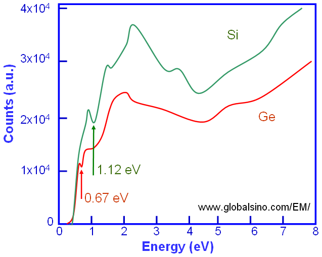
Figure 3441o. Schematic illustration of Si and Ge SSD spectra in the low-energy range.
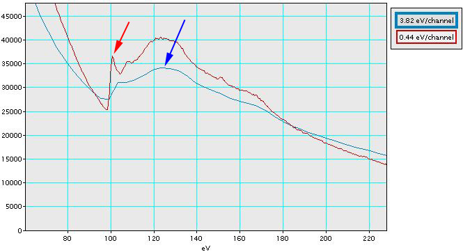
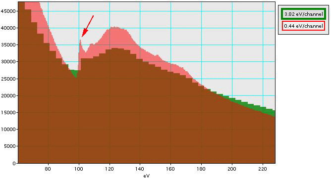
As an example of the binning effects on the energy resolution and the background of EEL spectra, the EELS of Si is shown in Figure 3441p. The two spectra were taken at energy dispersions of 0.44 eV/channel and 3.82 eV/channel, respectively. The full-width at half-maximum (FWHM) of the small peak marked by the red arrow is only 2 eV; however, the energy of each channel (pixel) with energy dispersion of 3.82 eV/channel is 3.82 eV. Therefore, such small peak is invisible even though the same EELS system and electron microscope are used for both spectra. Furthermore, the height of the peak marked by the blue arrow is smaller for the greater energy dispersion (3.82 eV/channel).
|
(a) |
|
(b) |
| Figure 3441p. EEL spectra of Si taken at energy dispersions of 0.44 eV/channel and 3.82 eV/channel, respectively. The two figures (a) and (b) present the same spectra, but in different format. Binning in a spectrum is performed by using greater energy dispersions. Here, 3.82 eV/channel is binning of 0.44 eV/channel by about 9x. |
|
[1] I. Sieber, R. Schneider, I. Doerfel, P. Schubert-Bischoff, S. Gall, W. Fuhs, Preparation of thin polycrystalline silicon films on glass by aluminium induced crystallisation—an electron microscopy study, Thin Solid Films 427 (2003) 298–302.
[2] Laurence A. J. Garvie, Alan J. Craven, Use of electron-energy loss near-edge fine structure in the study of minerals, American Mineralogist, 79, (1994) 411-425.
[3] M. Worch, H.J. Engelmann, W. Blum, E. Zschech, Cross-sectional thin film characterization of Si compounds in semiconductor device structures using both elemental and ELNES mapping by EFTEM, Thin Solid Films 405 (2002) 198–204.
[4] Koji Kimoto, Tomoko Sekiguchi and Takashi Aoyama, Chemical shift mapping of Si L and K edges using spatially resolved EELS and energy-filtering TEM, Journal of Electron Microscopy 46(5): 369-374 (1997).
[5] S. Pokrant, R. Pantel, M. Cheynet, Physical characterization by valence electron energy loss spectroscopy, 83 (11–12) 2364–2367 (2006).
[6] Kyle A. Brown and W. Ho, The interaction of methyl chloride and Si( 100) 2 x 1, Surface Science 338 (1995) 111-116.
[7] Mizoguchi T., Tanaka I., Mizuno M., Adachi H., Hashimoto T., Inui H., Yamaguchi M., Defect and electronic structure of TiSi2 thin films produced by co-sputterings. - Part II: Chemical bonding and electron energy-loss near-edge structures, Acta mater. 49 (2001) 2321–2328.
[8] Norihito Sakaguchi, Makito Miyake, Seiichi Watanabe, and Heishichiro Takahashi, EELS and Ab-Initio Study of Faceted CSL Boundary in Silicon, Materials Transactions, 52(3) (2011) 276.
|