Chapter/Index: Introduction | A | B | C | D | E | F | G | H | I | J | K | L | M | N | O | P | Q | R | S | T | U | V | W | X | Y | Z | Appendix
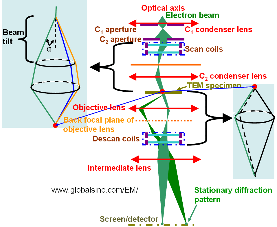
| The precession electron diffraction (PED) technique is a relatively new method and was proposed by Vincent and Midgley in 1994 [1]. The PED method is similar to the well-known X-ray (Buerger) precession technique [2]. However, it performs a precession movement of the primary electron beam around the microscope’s optical axis instead of that of a single crystal around a fixed primary X-ray beam direction. The PED technique has recently been developed rapidly mainly due to the availability of commercial and convenient setups. These setups can be implanted on most modern transmission electron microscopes (TEMs). The PED patterns look very similar to the SAED (conventional selected-area electron diffraction) patterns and micro-/nano- beam electron diffraction patterns. The main advantage of PED is to remove strong dynamical effects from the diffraction patterns and to provide more kinematical data, e.g. remove extra spots induced by dynamical effects. PED technique is close to hollow-cone diffraction technique but normally uses a parallel or nearly parallel incident electron beam. In PED technique, the electron beam is deflected twice. The electron beam first scans angularly around the optical axis on a pivot point, which is intersection point between the TEM optical axis and the specimen. The scan coils are normally deflection coils underneath the condenser lenses as shown in Figure 3906a. The diffraction pattern, located in the back focal plane of the objective lens, moves following the movement of the incident electron beam along the circumference of a circle. The movement diameter of diffraction pattern depends on the precession angle α. The primary electron beam and the diffracted beams are descanned (after they have left the specimen) in the same way that stationary diffraction patterns [3] are obtained in conventional TEMs. The beam deflection by the descan coils is exactly a compensation of the scan operation, meaning both scan and descan are simultaneously performed in order to stop the movement of diffraction pattern and to produce a stationary spot pattern on the screen or detector. The intensity of the diffraction spots is an integral over excitation error s. Different from hollow-cone diffraction technique, because PED works at the pivot point on the TEM sample, this technique can be used to perform local diffraction analysis at high spatial resolution, e.g. on nano-particles.
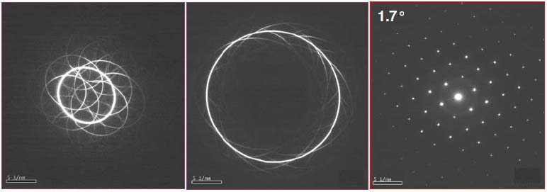
Figure 3906b presents patterns taken from a 40-nm thick silicon (Si) crystal close to the [110] orientation, showing the effects of scan coils and descan coils. In Figures 3906b (a) and (b), the fine arcs and circles are formed with pure scan or pure descan, respectively. Figure 3906b (c) shows a diffraction pattern with both proper scan and descan on, resulting in a stationary diffraction pattern.
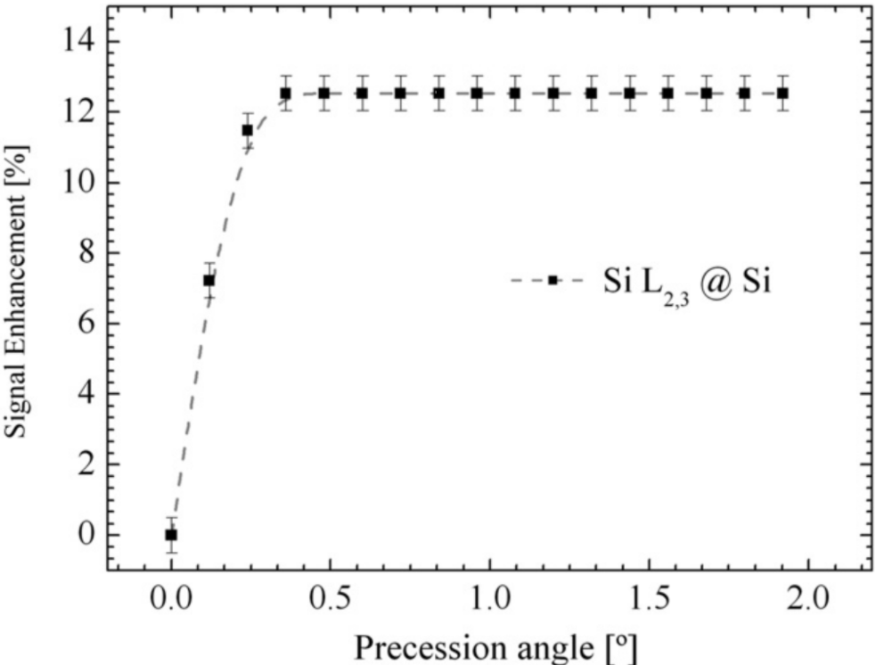
For symmetry determination with both XRD and electron diffraction crystallography, we are looking for symmetry-related reflections. Then, the difference between the two techniques is mainly on systematically forbidden reflections: Estrade et al. employed precession electron diffraction technique on EELS measurements and observed that the channeling effect is reduced with precession-on and thus the EELS signal is enhanced at non-zero angles and suturated at a precession angle of 0.5° (~9 mrad) as shown in Figure 3906c even though the TEM sample is aligned along a zone axis. The TEM sample thickness was 30 nm. This is reasonable because the electron beam is not really at the zone axis of the crystal of the TEM sample even though the optical axis is along the zone axis.
[1] R. Vincent, P.A. Midgley, Ultramicroscopy 53 (1994) 271.
|