=================================================================================
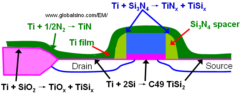
TiO2 TEM specimens can be prepared by crushing bulk single crystals into fine fragments in an agate mortar, dispersing in ethyl alcohol and finally by putting drops of ethyl alcohol on a carbon-film grid. [1]
Figure 2071a shows several chemical reactions occurring during annealing of a transistor structure coated with Ti to form a low resistive TiSi2 layer at the source, gate, and drain. When silicon and titanium are reacted, Ti and Si can diffuse laterally over the isolation regions and form thin filaments of TiSix that can electronically connect a gate electrode and source/drain regions and can cause failure of the device. This phenomenon is called "bridging". On the other hand, those by-products (TiSix, TiOx, and TiN) form over the isolation regions and cannot easily be etched in conventional salicide etching solutions. The use of a nitrogen atmosphere during thermal annealing is essential in preventing this failure mechanism [3] because nitrogen quickly diffuses into the grain boundaries and significantly suppresses any long-range silicon diffusion in the titanium layer. Furthermore, to avoid the by-product formation, the annealing temperature cannot be too high.
Figure 2071a. Several chemical reactions occurring during annealing of a transistor structure coated with Ti to form a low resistive SiTi2 layer.
Table 2071b. Properties of main crystalline TiO2.
|
|
|
|
TiO2 (B) |
TiO2, II |
TiO2, (H) |
Perovskite |
|
P42/mnm |
I41/amd |
Pbca |
C2/m |
Pbcn |
I4/m |
Pnma |
|
a = 0.459; c = 0.296 [1] |
a = 0.379; c = 0.951 |
a = 0.917; b = 0.546; c = 0.514 |
a = 1.216; b = 0.374; c = 0.651, β = 107.29° |
a = 0.452; b = 0.550; c = 0.494 |
a = 1.018; c = 0.297 |
a = 0.537; b = 0.764; c = 0.544 |
Unit cell |
|
|
|
|
|
|
|
Density (g/cm3) |
4.1 |
3.7 |
3.99 |
3.64 |
4.33 |
3.46 |
4.03 |
Specific weight |
4.2 |
3.9 |
2.87-4.01 |
|
|
|
|
Rockwell hardness |
6 - 6.5 |
5.5 - 6 |
5.5 - 6 |
|
|
|
|
Habitus |
Ditetragonal bipyramidal
|
Tetragonal bipyramidal tabular |
Bipyramidal rhombic |
|
|
|
|
Existing condition |
Stable: <1845 °C |
Metastable |
Metastable, rare |
|
|
|
|
Molecules per cell ( Z) |
2 |
4 |
8 |
|
|
|
|
|
6 |
6 |
6 |
|
|
|
|
Ti-O distance (Å) |
2 at 1.946
4 at 1.984 |
2 at 1.937
4 at 1.964 |
2 at 1.993
1 at 1.865
1 at 1.919
1 at 1.945
1 at 2.040 |
|
|
|
|
|
Ti: 0, 0, 0; 1/2, 1/2, 1/2.
O: 0.3, 0.3, 0; 0.8, 0.2, 1/2; 0.2, 0.8, 1/2; 0.7, 0.7, 0. |
|
|
|
|
|
|
Melting point (°C) |
1870 |
|
|
|
|
|
|
Boiling point (°C) |
2500-3000 |
2500-3000 |
|
|
|
|
|
|
Oxygen
deficiencies [2] |
|
|
|
|
|
|
Relaxation width of lattice at stacking faults
|
1 nm [1] |
|
|
|
|
|
|
Displacement vector R of stacking faults in (-101) plane |
-0.25±0.00, 0.00±0.03, -0.27±0.01 |
|
|
|
|
|
|
Band gap (eV) |
3.02 |
3.2 |
|
|
|
|
|
|
|
0 |
|
|
|
|
|
Static dielectric constant |
|
80 |
|
|
|
|
|
Absorption onset (nm) |
410 |
380 |
|
|
|
|
|
|
79.9 |
79.9 |
|
|
|
|
|
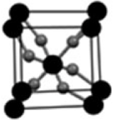
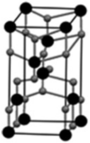
Table 2071c. Example of compounds with similar structures to BCC.
|
|
TiO2 (Rutile) |
|
|
Space group |
Im-3m |
P42/mnm |
Pm-3m |
Pn-3m |
Compounds |
α-Fe, W, Nb, Ta, Na, K, Mo, V |
GeO2, SnO2, PbO2 |
CsI, CsBr, CsCl |
Pb2O, Ag2O |
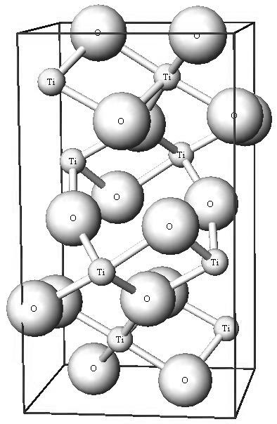
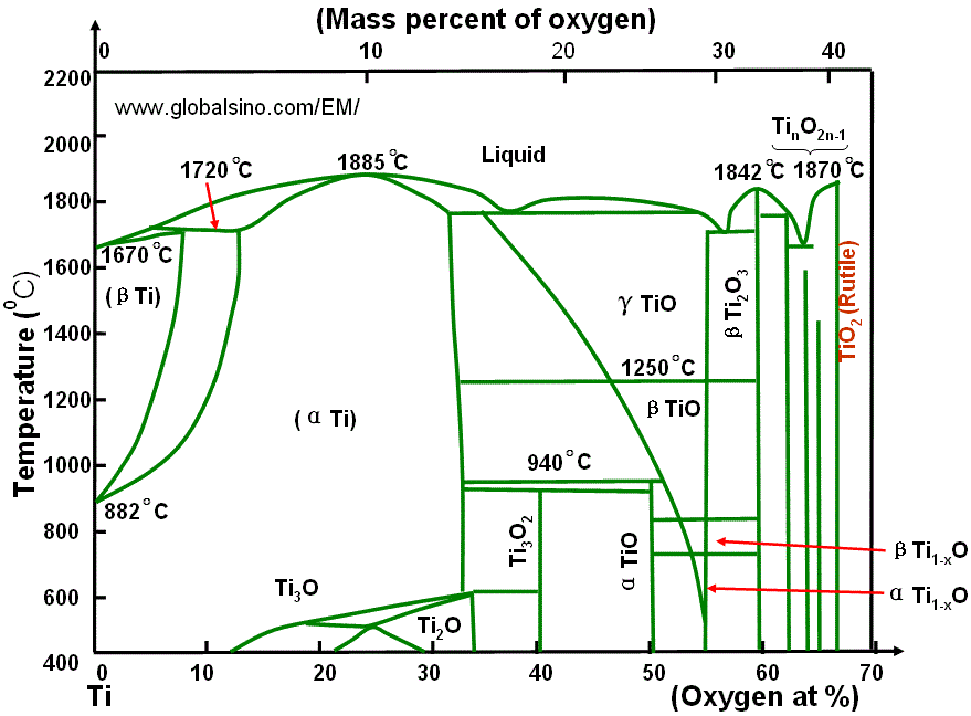
Figure 2071b. Ti-O phase diagram.
Table 2071d. Phases and space groups of TiOx.
Table 2071e. Other characteristics of TiO2 materials.
Most closed packed d-spacing and planes |
page1721 |
[1] Susumu Yamada and Michiyoshi Tanaka, Structure of a stacking fault in the (-101) plane of TiO2, Journal of Electron Microscopy 1: 67-74 (1997).
[2] Yamada S and Tanaka M (1995) Determination of the displacement vector at a stacking fault in TiO2 by convergent-beam electron diffraction. J. Electron Mkrosc 44: 212-218.
[3] C. K. Lau, “Method of Forming Titanium Disilicide,”
U.S. Patent 4,545,116, 1985.
|