Chapter/Index: Introduction | A | B | C | D | E | F | G | H | I | J | K | L | M | N | O | P | Q | R | S | T | U | V | W | X | Y | Z | Appendix
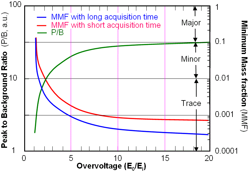
| In principle, low accelerating voltage electron beams can enhance the signals for both EELS and EDS because the reduced the acceleration voltage increases the ionization cross-section, which is determined by the overvoltage ratio. However, similar to EELS measurements, when the accelerating voltage of the electron beam increases, the intensity of the characteristic X-ray slightly decreases (see page4646), but the background X-ray decreases significantly due to less multiple scatterings, and thus the peak-to-background ratio (P/B ratio) in EDS practically increases with the accelerating voltages, especially from 100 kV to 400 kV, resulting in an increase in the detection sensitivity of any trace elements. The Peak to Background Ratio (P/B) of EDS measurements is given by, Equation 4606a indicates the best P/B would occur at the highest energy of the incident beam. This can be true for TEM-EDS measurements with thin specimens. However, in practical SEM measurements with bulk samples, an overvoltage of 1.5 - 3 is normally a good compromise in order to obtain good spatial resolution and to minimize the absorption of X-rays. On the other hand, the peak to background ratios (P/B) are better with higher take-off angles. In general, Figure 4606a shows the behavior of peak-to-background ratio and minimum mass fraction (detection limit) as a function of overvoltage. For effective generation of X-ray by ionization processed by electron interaction, the overvoltage U should be greater than 1.3 because the X-ray peak to background ratio (P/B) of X-ray signal is reduced substantially as E0 (energy of incident beam) approaches Ei. It is necessary to mention that the low energy X-ray lines, e.g. Cu(L) at 0.93 keV instead of Cu(K) at 8.04 keV, are used at low accelerating voltage of incident electrons.
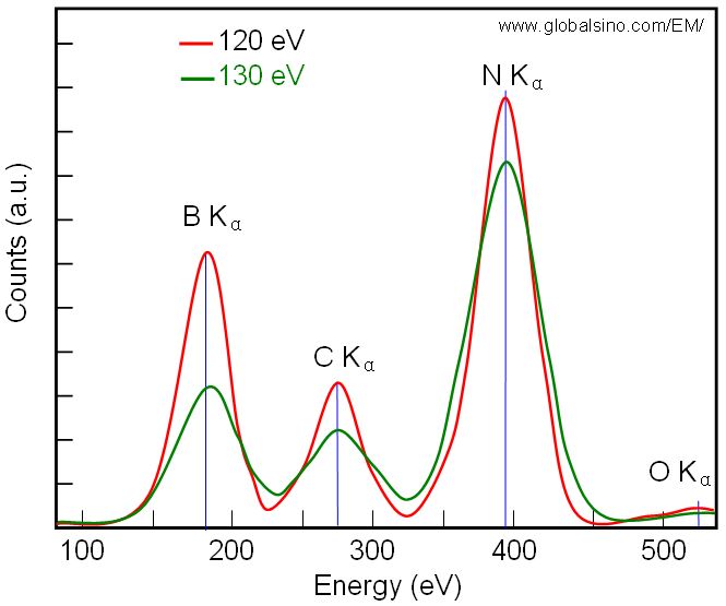
Furthermore, there are many drawbacks induced by the specimen contamination in EM analysis, for instance: Quantitative analysis based on EDS method can be done by the following procedure: In practical SEM-EDS quantification, matrix correction on EDS software takes into account the atomic number effects, absorption effects and secondary fluorescence effects. The local peak to background (P/B) ratios are then input into the modified ZAF matrix correction. In this case, the P/B-ZAF analysis is normally self-calibrating. Because the EDS peaks are so broad, their Gaussian tails extend over a substantial energy range, interfering with the adjacent background. Therefore, the background measurements are difficult. For a material with multiple chemical elements, the spectrum becomes more complex, and thus the quantification and interpretation is less accurate. In general, EDS has relatively low peak-to-background ratio in electron microscopes due to the high background coming from bremsstrahlung radiation emitted by electrons suffering deceleration on scattering by atoms. Figure 4606b shows two schematic spectra obtained from two EDS detectors with energy resolutions at Mn Kα 120 eV and 130 eV, respectively. It is clear that higher spectrum peak can be obtained with better resolution. Consequently, the higher peak improves the peak-to-background ratio and facilitates the spectrum deconvolution.
Table 4606. Examples of signal-to-background (S/B) ratios in EDS.
|